30V, 105A,RDS(ON) = 6mΩ @VGS = 10V. RDS(ON) = 8mΩ @VGS = 4.5V. Super high dense cell design for extremely low RDS(ON). High power and current handing capability. Lead free product is acquired. TO-220 & TO-263 package. D
G S
CEB SERIES TO-263(DD-PAK)
G D S
CEP SERIES TO-220
G
D S.
Full PDF Text Transcription for CEB3060 (Reference)
Note: Below is a high-fidelity text extraction (approx. 800 characters) for
CEB3060. For precise diagrams, and layout, please refer to the original PDF.
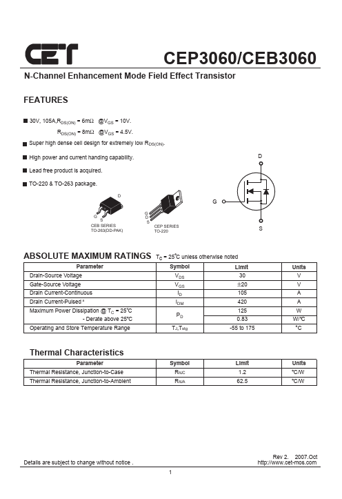
CEP3060/CEB3060 N-Channel Enhancement Mode Field Effect Transistor FEATURES 30V, 105A,RDS(ON) = 6mΩ @VGS = 10V. RDS(ON) = 8mΩ @VGS = 4.5V. Super high dense cell design fo...
View more extracted text
@VGS = 10V. RDS(ON) = 8mΩ @VGS = 4.5V. Super high dense cell design for extremely low RDS(ON). High power and current handing capability. Lead free product is acquired. TO-220 & TO-263 package. D G S CEB SERIES TO-263(DD-PAK) G D S CEP SERIES TO-220 G D S ABSOLUTE MAXIMUM RATINGS Tc = 25 C unless otherwise noted Parameter Symbol Limit Drain-Source Voltage Gate-Source Voltage Drain Current-Continuous Drain Current-Pulsed a Maximum Power Dissipation @ TC = 25 C - Derate above 25 C VDS VGS ID IDM PD 30 ±20 105 420 125 0.