-30V, -35A, RDS(ON) =36mΩ @VGS = -10V. RDS(ON) =57mΩ @VGS = -5V. Super high dense cell design for extremely low RDS(ON). High power and current handing capability. Lead free product is acquired. TO-220 & TO-263 package. D
D
G
S CEB SERIES TO-263(DD-PAK) G
G D S
CEP SERIES TO-220
S.
Full PDF Text Transcription for CEB35P03 (Reference)
Note: Below is a high-fidelity text extraction (approx. 800 characters) for
CEB35P03. For precise diagrams, and layout, please refer to the original PDF.
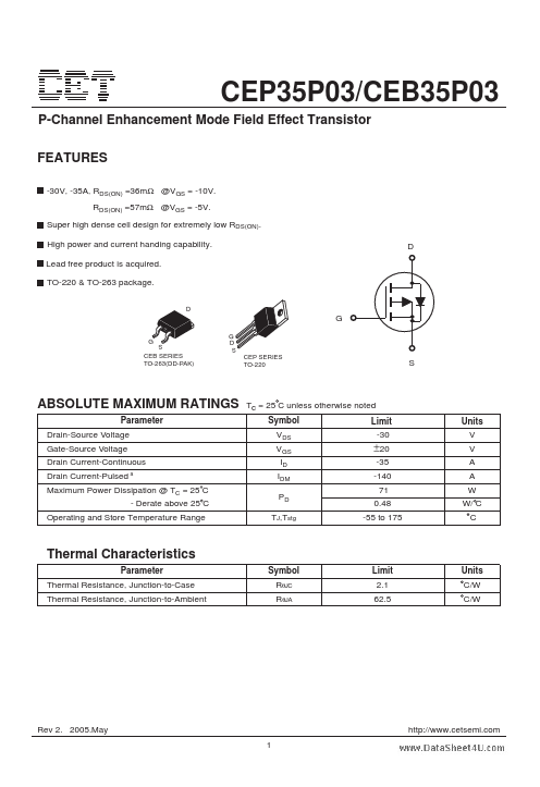
CEP35P03/CEB35P03 P-Channel Enhancement Mode Field Effect Transistor FEATURES -30V, -35A, RDS(ON) =36mΩ @VGS = -10V. RDS(ON) =57mΩ @VGS = -5V. Super high dense cell desig...
View more extracted text
6mΩ @VGS = -10V. RDS(ON) =57mΩ @VGS = -5V. Super high dense cell design for extremely low RDS(ON). High power and current handing capability. Lead free product is acquired. TO-220 & TO-263 package. D D G S CEB SERIES TO-263(DD-PAK) G G D S CEP SERIES TO-220 S ABSOLUTE MAXIMUM RATINGS Parameter Drain-Source Voltage Gate-Source Voltage Drain Current-Continuous Drain Current-Pulsed a Tc = 25 C unless otherwise noted Symbol Limit VDS VGS ID IDM PD TJ,Tstg -30 Units V V A A W W/ C C ±20 -35 -140 71 0.