Datasheet4U Logo Datasheet4U.com

CEB35P10 - P-Channel MOSFET

Key Features

  • -100V, -32A, RDS(ON) =76mΩ @VGS = -10V. RDS(ON) =92mΩ @VGS = -4.5V. Super high dense cell design for extremely low RDS(ON). High power and current handing capability. Lead-free plating ; RoHS compliant. TO-220 & TO-263 package. D G S CEB SERIES TO-263(DD-PAK) G D S CEP SERIES TO-220 G D S.

📥 Download Datasheet

Datasheet Details

Part number CEB35P10
Manufacturer CET
File Size 377.40 KB
Description P-Channel MOSFET
Datasheet download datasheet CEB35P10 Datasheet

Full PDF Text Transcription for CEB35P10 (Reference)

Note: Below is a high-fidelity text extraction (approx. 800 characters) for CEB35P10. For precise diagrams, and layout, please refer to the original PDF.

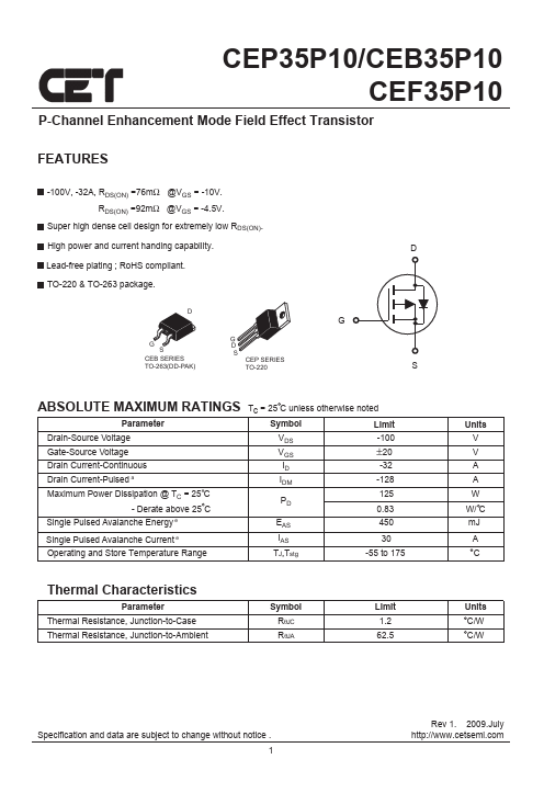
CEP35P10/CEB35P10 CEF35P10 P-Channel Enhancement Mode Field Effect Transistor FEATURES -100V, -32A, RDS(ON) =76mΩ @VGS = -10V. RDS(ON) =92mΩ @VGS = -4.5V. Super high dens...

View more extracted text
RDS(ON) =76mΩ @VGS = -10V. RDS(ON) =92mΩ @VGS = -4.5V. Super high dense cell design for extremely low RDS(ON). High power and current handing capability. Lead-free plating ; RoHS compliant. TO-220 & TO-263 package. D G S CEB SERIES TO-263(DD-PAK) G D S CEP SERIES TO-220 G D S ABSOLUTE MAXIMUM RATINGS Tc = 25 C unless otherwise noted Parameter Symbol Limit Drain-Source Voltage Gate-Source Voltage VDS -100 VGS ±20 Drain Current-Continuous Drain Current-Pulsed a ID -32 IDM -128 Maximum Power Dissipation @ TC = 25 C - Derate above 25 C PD 125 0.