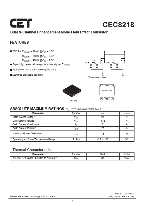
Click to expand full text
CEC8218
Dual N-Channel Enhancement Mode Field Effect Transistor
FEATURES
20V, 7A, RDS(ON) = 20mΩ @VGS = 4.5V. RDS(ON) = 28mΩ @VGS = 2.5V. RDS(ON) = 48mΩ @VGS = 1.8V.
Super High dense cell design for extremely low RDS(ON). High power and current handing capability. Lead free product is acquired.
D
*1K G1
*1K G2
S1 *Typical value by design
5 67 8 Bottom View
DFN3*3
4 321
ABSOLUTE MAXIMUM RATINGS TA = 25 C unless otherwise noted
Parameter
Symbol
Limit
Drain-Source Voltage Gate-Source Voltage
VDS 20
VGS ±12
Drain Current-Continuous Drain Current-Pulsed a
ID 7 IDM 28
Maximum Power Dissipation
PD 1.