CED55N10
Key Features
- Super high dense cell design for extremely low RDS(ON)
- High power and current handing capability
- Lead-free plating ; RoHS pliant
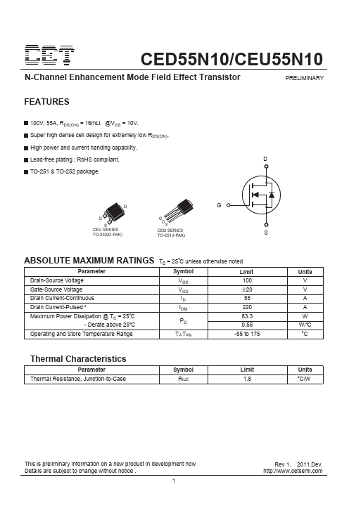
- TO-251 & TO-252 package
- D D G S CEU SERIES TO-252(D-PAK) G DS CED SERIES TO-251(I-PAK) G S