Datasheet4U.com
🌙
CED71A3 Datasheet | CET
Part:
CED71A3
Description:
N-Channel MOSFET
Category:
MOSFET
Manufacturer:
CET
Size:
60.96 KB
CED71A3 Datasheet (PDF) Download
CET
CED71A3
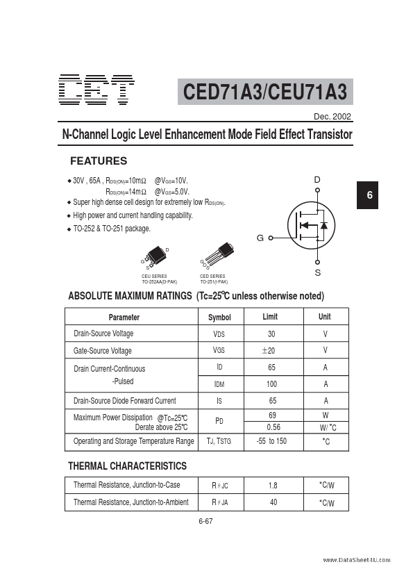
Key Features
RDS(ON)=14m Ω @VGS=5.0V
Super high dense cell design for extremely low RDS(ON)
High power and current handling capability
TO-252 & TO-251 package
D 6 G D G S G D S CEU SERIES TO-252AA(D-PAK) CED SERIES TO-251(l-PAK) S
×
Close