Click to expand full text
CEF02N6
Sep. 2002
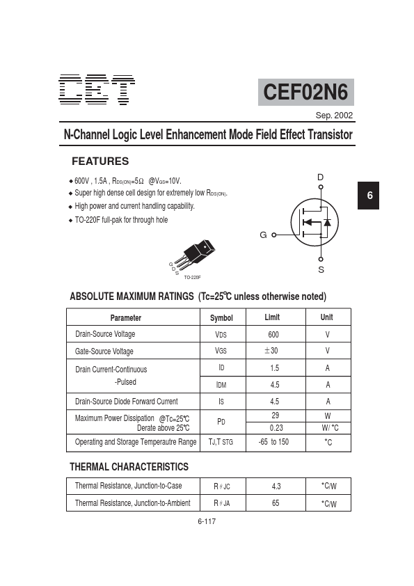
N-Channel Logic Level Enhancement Mode Field Effect Transistor
FEATURES
600V , 1.5A , RDS(ON)=5 Ω @VGS=10V. Super high dense cell design for extremely low RDS(ON). High power and current handling capability. TO-220F full-pak for through hole
D
6
G
G D S
S
TO-220F
ABSOLUTE MAXIMUM RATINGS (Tc=25 C unless otherwise noted)
Parameter Drain-Source Voltage Gate-Source Voltage Drain Current-Continuous -Pulsed Drain-Source Diode Forward Current Maximum Power Dissipation @Tc=25 C Derate above 25 C Operating and Storage Temperautre Range Symbol VDS VGS ID IDM IS PD TJ,T STG Limit 600 Unit V V A A A W W/ C C
Ć 30
1.5 4.5 4.5 29 0.23 -65 to 150
THERMAL CHARACTERISTICS
Thermal Resistance, Junction-to-Case Thermal Resistance, Junction-to-Ambient RįJC RįJA
6-117
4.