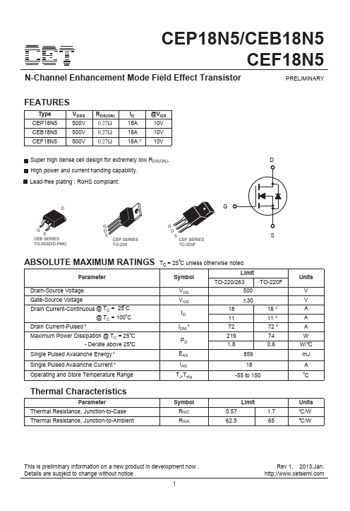
Click to expand full text
CEP18N5/CEB18N5
CEF18N5
N-Channel Enhancement Mode Field Effect Transistor
PRELIMINARY
FEATURES
Type CEP18N5 CEB18N5 CEF18N5
VDSS 500V 500V
500V
RDS(ON) 0.27Ω 0.27Ω
0.27Ω
ID 18A 18A 18A d
@VGS 10V 10V
10V
Super high dense cell design for extremely low RDS(ON). High power and current handing capability. Lead-free plating ; RoHS compliant.
D
DG
G S
CEB SERIES TO-263(DD-PAK)
G D S
CEP SERIES TO-220
G
D S CEF SERIES
TO-220F
S
ABSOLUTE MAXIMUM RATINGS Tc = 25 C unless otherwise noted
Parameter
Symbol
Limit
TO-220/263
TO-220F
Drain-Source Voltage
Gate-Source Voltage Drain Current-Continuous @ TC = 25 C
@ TC = 100 C Drain Current-Pulsed a
Maximum Power Dissipation @ TC = 25 C - Derate above 25 C
VDS VGS ID
IDM e
PD
500
±30
18 11 72 219 1.8
18 d 11 d 72 d 74 0.