CEM3501L Overview
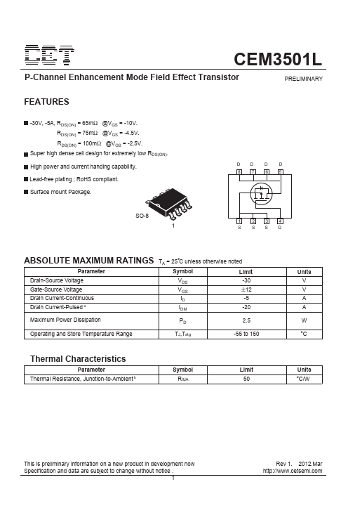
CEM3501L P-Channel Enhancement Mode Field Effect Transistor PRELIMINARY.
CEM3501L Key Features
- 30V, -5A, RDS(ON) = 65mΩ @VGS = -10V. RDS(ON) = 75mΩ @VGS = -4.5V. RDS(ON) = 100mΩ @VGS = -2.5V
CEM3501L datasheet by CET.
| Part number | CEM3501L |
|---|---|
| Datasheet | CEM3501L-CET.pdf |
| File Size | 387.77 KB |
| Manufacturer | CET |
| Description | p- |
|
|
CEM3501L P-Channel Enhancement Mode Field Effect Transistor PRELIMINARY.
| Part Number | Description |
|---|---|
| CEM3053 | P-Channel MOSFET |
| CEM3060 | N-Channel Enhancement Mode Field Effect Transistor |
| CEM3082 | N-Channel Enhancement Mode Field Effect Transistor |
| CEM3083 | P-Channel MOSFET |
| CEM3109 | Dual MOSFET |
| CEM3120 | N-Channel Enhancement Mode Field Effect Transistor |
| CEM3128 | Dual N-Channel Enhancement Mode Field Effect Transistor |
| CEM3138 | Dual N-Channel Enhancement Mode Field Effect Transistor |
| CEM3172 | N-Channel Enhancement Mode Field Effect Transistor |
| CEM3178 | Dual N-Channel Enhancement Mode Field Effect Transistor |