Datasheet Summary
CEP02N65G/CEB02N65G CEF02N65G
N-Channel Enhancement Mode Field Effect Transistor
Features
Type CEP02N65G CEB02N65G CEF02N65G
VDSS 650V 650V
650V
RDS(ON) 5.5Ω 5.5Ω
5.5Ω
ID @VGS 2A 10V 2A 10V 2A d 10V
Super high dense cell design for extremely low RDS(ON). High power and current handing capability. Lead free product is acquired.
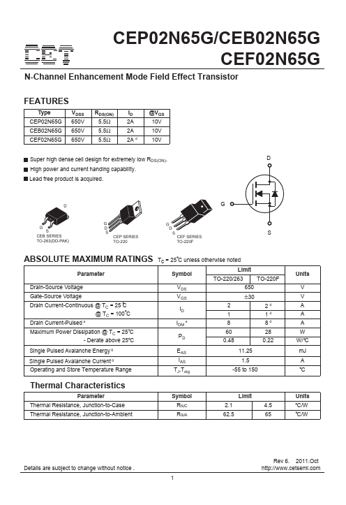
CEB SERIES TO-263(DD-PAK)
CEP SERIES TO-220
D S CEF...