Datasheet4U.com
🌙
CET3301 Datasheet | CET
Part:
CET3301
Description:
P-Channel MOSFET
Category:
MOSFET
Manufacturer:
CET
Size:
425.31 KB
CET3301 Datasheet (PDF) Download
CET
CET3301
Key Features
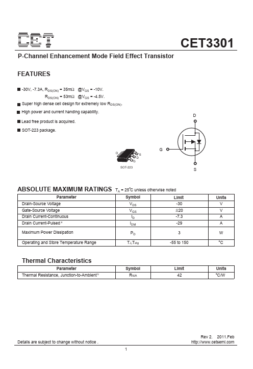
G SOT-223 G S
×
Close