CMX90B702
CMX90B702 is Low Current/Noise Gain Block manufactured by CML.
Description
The CMX90B702 is a low-current 50 Ω gain block suitable for a wide variety of wireless applications covering 23
- 29.5 GHz.
CMX90B702 is highly integrated to minimize external ponent count and board area. RF ports are matched on-chip to 50 Ω with an output DC-blocking capacitor. An active bias circuit helps maintain performance over a wide temperature range and supply voltage of 3
- 5 V.
The device is an easy-to-use gain block with fast enable circuit and dual-bias mode for system optimization, selecting bias of 10 m A or 15 m A.
CMX90B702 is fabricated using a Ga As p HEMT process to provide optimum gain, linearity, and noise together with low DC power consumption.
A footprint-patible variant, CMX90B701, is available for applications covering 17
- 23 GHz.
Applications
- 5G mm Wave Infrastructure
- Sat (K and Ka band)
- Microwave Backhaul
- Fixed Wireless Access (FWA)
- 24 GHz ISM band
3x3mm VQFN-16 Package
Product Features
- Frequency range 23
- 29.5 GHz
- Small signal gain 17.5 d B
- Single positive DC supply 3
- 5 V
- Low power consumption 40 m W
- Output P1d B +5 d Bm @ 26 GHz
- Output IP3 +15 d Bm @ 26 GHz
- Noise figure 4 d B
- Dual-bias mode (low/high setting)
- 105 °C operating temperature
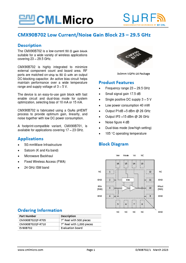
Block Diagram
Ven Mode Vd NC
16 15 14 13
2 bias
RFin (50Ω)
RFout (50Ω)
Ordering Information
Part Number CMX90B702QF-R705 CMX90B702QF-R710...