Overview: CL12464FF LVDS Receiver 24bit FPD-link 85MHz Introduction
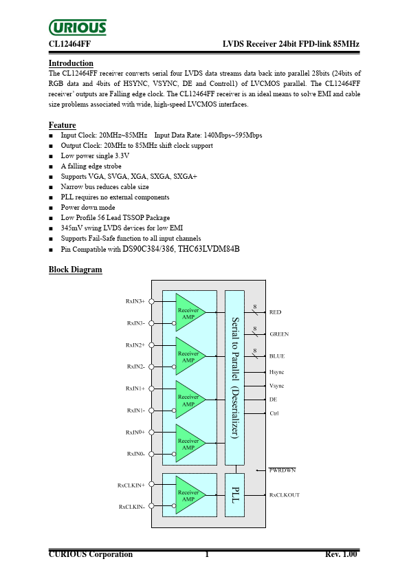
The CL12464FF receiver converts serial four LVDS data streams data back into parallel 28bits (24bits of RGB data and 4bits of HSYNC, VSYNC, DE and Control1) of LVCMOS parallel. The CL12464FF receiver’ outputs are Falling edge clock. The CL12464FF receiver is an ideal means to solve EMI and cable size problems associated with wide, high-speed LVCMOS interfaces. Feature
■ Input Clock: 20MHz~85MHz Input Data Rate: 140Mbps~595Mbps ■ Output Clock: 20MHz to 85MHz shift clock support ■ Low power single 3.3V ■ A falling edge strobe ■ Supports VGA, SVGA, XGA, SXGA, SXGA+ ■ Narrow bus reduces cable size ■ PLL requires no external ponents ■ Power down mode ■ Low Profile 56 Lead TSSOP Package ■ 345mV swing LVDS devices for low EMI ■ Supports Fail-Safe function to all input channels
■ Pin patible with DS90C384/386, THC63LVDM84B Block Diagram CURIOUS Corporation 1 Rev. 1.00 CL12464FF Pin Configuration 1 RxOUT22 2 RxOUT23 3 RxOUT24 GND 4 5 RxOUT25 6 RxOUT26 7 RxOUT27 8 LVDS GND RxIN0- 9 RxIN0+ 10 RxIN1- 11 RxIN1+ 12 13 LVDS Vcc 14 LVDS GND RxIN2- 15 RxIN2+ 16 17 RxCLKIN- 18 RxCLKIN+ RxIN3- 19 RxIN3+ 20 21 LVDS GND 22 PLL GND PLL Vcc 23 24 PLL GND 25 Power Down 26 RxCLKOUT RxOUT0 27 GND 28 CL12464FF LVDS Receiver 24bit FPD-link 85MHz
56 Vcc 55 RxOUT21 54 RxOUT20 53 RxOUT19 52 GND 51 RxOUT18 50 RxOUT17 49 RxOUT16 48 Vcc 47 RxOUT15 46 RxOUT14 45 RxOUT13 44 GND 43 RxOUT12 42 RxOUT11 41 RxOUT10 40 Vcc 39 RxOUT9 38 RxOUT8 37 RxOUT7 36 GND 35 RxOUT6 34 RxOUT5 33 RxOUT4 32 RxOUT3 31 Vcc 30 RxOUT2 29 RxOUT1 CURIOUS Corporation 2 Rev. 1.