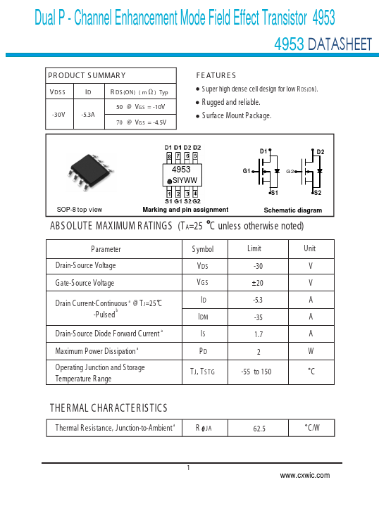
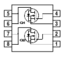
Click to expand full text
Dual P - Channel Enhancement Mode Field Effect Transistor 4953
4953 DATASHEET
P R ODUC T S UMMAR Y
VDS S -30V
ID -5.3A
R DS (ON) ( m Ω ) Typ
50 @ VG S = -10V 70 @ VG S = -4.5V
F E AT UR E S S uper high dense cell design for low R DS(ON).
R ugged and reliable. S urface Mount P ackage.
D1 D2
4953
SIYWW
G1 G2 S1 S2
SOP-8 top view
Marking and pin assignment
Schematic diagram
ABS OLUTE MAXIMUM R ATINGS (TA=25 C unless otherwise noted)
P arameter Drain-S ource Voltage
Gate-S ource Voltage
Drain C urrent-C ontinuous a @ TJ=25 C -P ulsed b
Drain-S ource Diode Forward C urrent a Maximum P ower Dissipation a Operating Junction and S torage Temperature R ange
S ymbol VDS VGS ID IDM IS PD
TJ, TSTG
Limit -30 20 -5.3 -35 1.