GENERAL DESCRIPTION
Based on current mode control and simplified the design of loop compensation. Additional features include: error amplifier, precision reference, cycle-by- cycle over-current protection, slope compensation, soft-start, oscillator synchronization capability, and thermal shutdown. ABSOLUTE MAXIMUM RATINGS
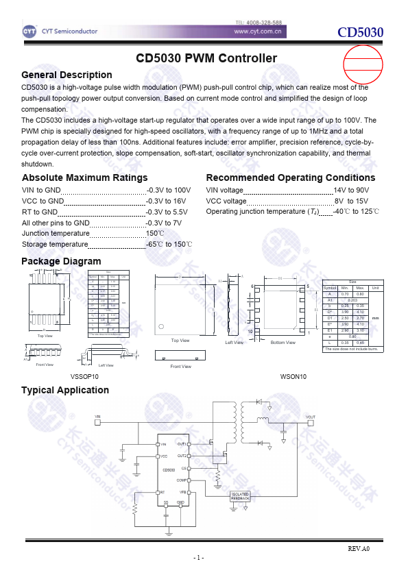
Recommended Operating Conditions VIN to GND -0.3V to 100V VIN voltage 14V to 90V VCC to GND RT to GND All other pins to GND Junction temperature -0.3V to 16V -0.3V to 5.5V -0.3V to 7V 150℃ VCC voltage Operating junction temperature (TJ) 8V to 15V -40℃ to 125℃ Storage temperature -65℃ to 150℃ Package Diagram e b E HE D Top View Size Symbol Min. Max. Unit A -- 1.10 A1 0.02 0.15 b 0.17 0.33 c 0.09 0.23 Da 2.90 3.10 mm Ea 2.90 3.10 e 0.50 HE 4.70 5.10 LP 0.40 0.80 L 0.95 θ 0 8 ° a The size dose not include burrs. A A1 Front View LP θ c L Left View VSSOP10 Typical Application D Top View Front View A A1 6 b E e 10 L Left View D1 Bottom View Size 5 Symbol Min. Max. Unit A 0.70 0.8 0 A1 0.203 b 0.25 0.35 E1 Da 3.9 0 4.1 0 D1 2.50 2.70 mm Ea 3.9 0 4.1 0 1 E1 2.90 3.10 e 0.80 L 0.35 0.45 a The size dose not include burrs. CYT