FEATURES
n n n GENERAL DESCRIPTION
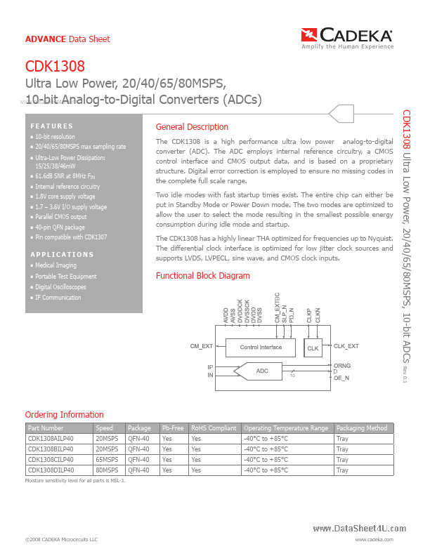
Digital error correction is employed to ensure no missing codes in the complete full scale range. Two idle modes with fast startup times exist. The two modes are optimized to allow the user to select the mode resulting in the smallest possible energy consumption during idle mode and startup. The CDK1308 has a highly linear THA optimized for frequencies up to Nyquist. The differential clock interface is optimized for low jitter clock sources and supports LVDS, LVPECL, sine wave, and CMOS clock inputs. 10-bit resolution 20/40/65/80MSPS max sampling rate Ultra-Low Power Dissipation: 15/25/38/46mW n n n n n n n 61.6dB SNR at 8MHz FIN Internal reference circuitry 1.8V core supply voltage 1.7 – 3.6V I/O supply voltage Parallel CMOS output 40-pin QFN package Pin compatible with CDK1307 APPLICATIONS
n n n n Medical Imaging Portable Test Equipment Digital Oscilloscopes IF Communication Functional Block Diagram Rev 0.1 10 Ordering Information Part Number CDK130... Cadeka