CDK8307
CDK8307 is Ultra Low Power ADC manufactured by Cadeka.
PRELIMINARY Data Sheet
A m p l i fy t h e H u m a n E x p e r i e n c e
12/13-bit, 20/40/50/65MSPS, Eight Channel, .. Ultra Low Power ADC with LVDS
Features n n
CDK8307 12/13-bit, 20/40/50/65MSPS, Eight Channel, Ultra Low Power ADC with LVDS
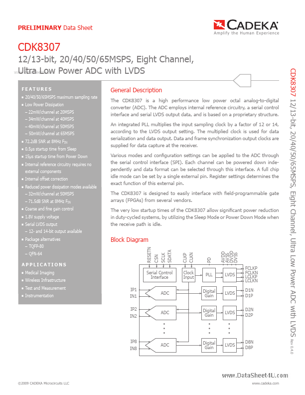
General Description
The CDK8307 is a high performance low power octal analog-to-digital converter (ADC). The ADC employs internal reference circuitry, a serial control interface and serial LVDS output data, and is based on a proprietary structure. An integrated PLL multiplies the input sampling clock by a factor of 12 or 14, according to the LVDS output setting. The multiplied clock is used for data serialization and data output. Data and frame synchronization output clocks are supplied for data capture at the receiver. Various modes and configuration settings can be applied to the ADC through the serial control interface (SPI). Each channel can be powered down independently and data format can be selected through this interface. A full chip idle mode can be set by a single external pin. Register settings determines the exact function of this external pin. The CDK8307 is designed to easily interface with field-programmable gate arrays (FPGAs) from several vendors. The very low startup times of the CDK8307 allow significant power reduction in duty-cycled systems, by utilizing the Sleep Mode or Power Down Mode when the receive path is idle.
20/40/50/65MSPS maximum sampling rate Low Power Dissipation
- 22m W/channel at 20MSPS
- 34m W/channel at 40MSPS
- 40m W/channel at 50MSPS
- 50m W/channel at 65MSPS n n n n
72.2d B SNR at 8MHz FIN 0.5μs startup time from Sleep 15μs startup time from Power Down Internal reference circuitry requires no Internal offset correction Reduced power dissipation modes available
external ponents n n
- 32m W/channel at 50MSPS
- 71.5d B SNR at 8MHz FIN n n n
Coarse and fine gain control 1.8V supply voltage Serial LVDS output Package...