SST270
SST270 is P-Channel JFET manufactured by Calogic.
FEATURES
DESCRIPTION
The J270/SST270 Series is an all-purpose amplifier for designs requiring P-channel operation. These devices feature high gain, low noise and tight VGS(OFF) limits for simple circuit design. They are available in low-cost SOT-23 and TO-92 packages and are fully patible with automatic insertion techniques. ORDERING INFORMATION Part J270-271 SST270-271 Package Plastic TO-92 Plastic SOT-23 Temperature Range -55o C to +135o C -55o C to +135o C
- Surface Mount
- P-Channel Amplifier
APPLICATIONS
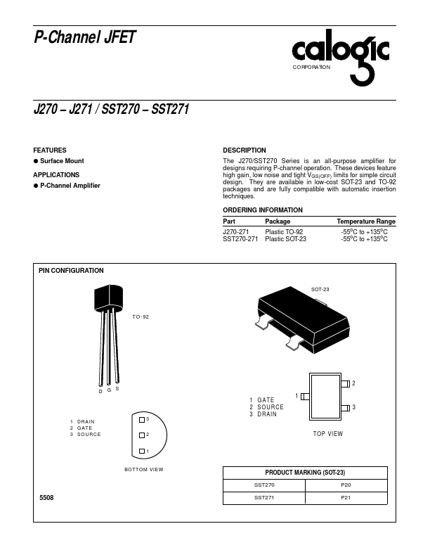
PIN CONFIGURATION
SOT-23
- 92
2 1 GATE 2 SOURCE 3 D RA IN
1 D RA IN 2 GATE 3 SOURCE
3 2 1
TOP VIEW
BOTTOM VIEW
PRODUCT MARKING (SOT-23) SST270 P20 P21
SST271
J270
- J271 / SST270
- SST271
CORPORATION
ABSOLUTE MAXIMUM RATINGS (TA = 25o C unless otherwise noted) PARAMETERS/TEST CONDITIONS Gate-Drain Voltage Gate-Source Voltage Gate Current Power Dissipation Power Derating Operating Junction Temperature Storage Temperature Lead Temperature (1/16" from case for 10 seconds) SYMBOL VGD VGS IG PD TJ Tstg TL LIMIT 30 30 -50 350 2.8 -55 to 150 -55 to 150 300 UNIT V V m A m W m W/ o C o C o C o C
ELECTRICAL CHARACTERISTICS (TA = 25o C unless otherwise noted)
SYMBOL STATIC V(BR)GSS VGS(OFF ) IDSS IGSS IG VGS(F) DYNAMIC gfs gos Ciss Crss mon-Source Forward Transconductance mon-Source Output Conductance mon-Source Input Capacitance mon-Source Reverse Transfer Capacitance Equivalent Input Noise Voltage 20 p F 4 n V √ Hz VDS = -15V, VGS = 0V f = 1MHz 6 15 200 8 18 500 m S VDS = -15V, VGS = 0V f = 1k Hz µS Gate-Source Breakdown Voltage Gate-Source Cutoff Voltage Saturation Drain Current Gate Reverse Current 5 Gate Operating Current Gate-Source Forward Voltage 10 -0.7 n A p A V TA = 125 o C VDG = -15V, I D = -1m A IG = -1m A, VDS = 0V
PARAMETER
TYP1
270 MIN MAX
271 UNIT MIN MAX TEST CONDITIONS
30 0.5 -2 2.0 -15 200
30 V 1.5 -6 4.5 -50 200 m A p A
IG = 1 µA, VDS = 0V VDS = -15V, ID = -1n A VDS = -15V, VGS = 0V VGS = 20V, VDS = 0V
10 en
VDS =...