FEATURES
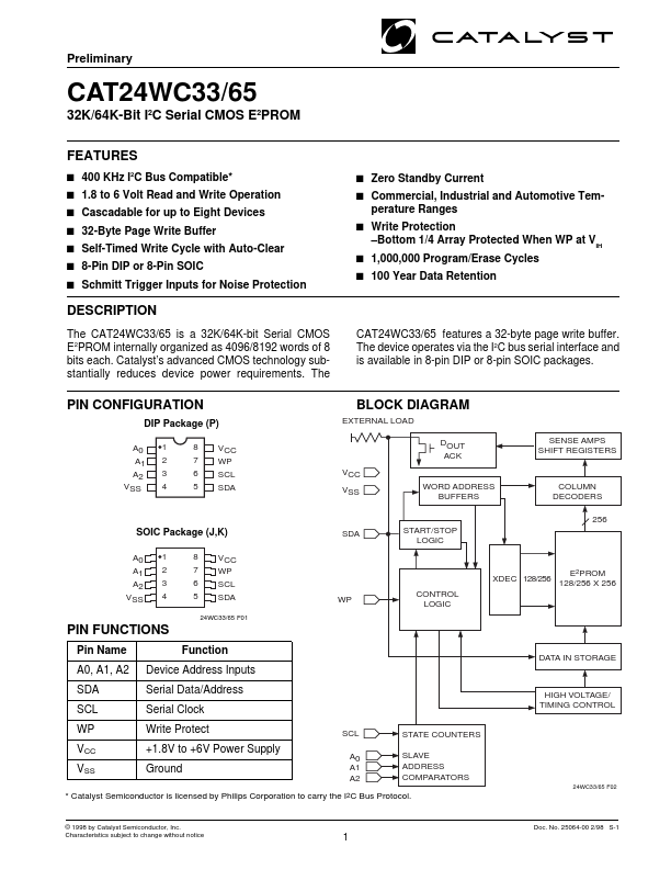
s 400 KHz I2C Bus Compatible* s 1.8 to 6 Volt Read and Write Operation s Cascadable for up to Eight Devices s 32-Byte Page Write Buffer s Self-Timed Write Cycle with Auto-Clear s 8-Pin DIP or 8-Pin SOIC s Schmitt Trigger Inputs for Noise Protection s Zero Standby Current s Commercial, Industrial and Automotive Tem- perature Ranges s Write Protection –Bottom 1/4 Array Protected When WP at VIH s 1,000,000 Program/Erase Cycles s 100 Year Data Retention DESCRIPTION
Catalyst’s advanced CMOS technology substantially reduces device power requirements. PIN CONFIGURATION DIP Package (P) A0 A1 A2 VSS 1 2 3 4 8 7 6 5 VCC WP SCL SDA BLOCK DIAGRAM EXTERNAL LOAD DOUT ACK VCC VSS WORD ADDRESS BUFFERS COLUMN DECODERS 256 SENSE AMPS SHIFT REGISTERS SOIC Package (J,K) A0 A1 A2 VSS 1 2 3 4 8 7 6 5 VCC WP SCL SDA 24WC33/65 F01 SDA START/STOP LOGIC E2PROM XDEC 128/256 128/256 X 256 WP CONTROL LOGIC PIN FUNCTIONS Pin Name A0, A1, A2 SDA SCL WP VCC VSS Function Device Address Inputs Serial Data/Addr... Catalyst Semiconductor