CAT25C05
CAT25C05 is 1K/2K/4K/8K/16K SPI Serial CMOS EEPROM manufactured by Catalyst Semiconductor.
- Part of the CAT25C11 comparator family.
- Part of the CAT25C11 comparator family.
CAT25C11/03/05/09/17
1K/2K/4K/8K/16K SPI Serial CMOS EEPROM Features s 10 MHz SPI patible s 1.8 to 6.0 volt operation s Hardware and software protection s Low power CMOS technology s SPI modes (0,0 & 1,1)- s mercial, industrial, automotive and extended s 1,000,000 program/erase cycles s 100 year data retention s Self-timed write cycle s 8-pin DIP/SOIC, 8-pin TSSOP and 8-pin MSOP s 16/32-byte page write buffer s Write protection temperature ranges
- Protect first page, last page, any 1/4 array or lower 1/2 array
DESCRIPTION
The CAT25C11/03/05/09/17 is a 1K/2K/4K/8K/16K-Bit SPI Serial CMOS EEPROM internally organized as 128x8/256x8/512x8/1024x8/2048x8 bits. Catalyst’s advanced CMOS Technology substantially reduces device power requirements. The CAT25C11/03/05 Features a 16-byte page write buffer. The 25C09/17 Features a 32-byte page write buffer.The device operates via the SPI bus serial interface and is enabled though a Chip Select (CS). In addition to the Chip Select, the clock
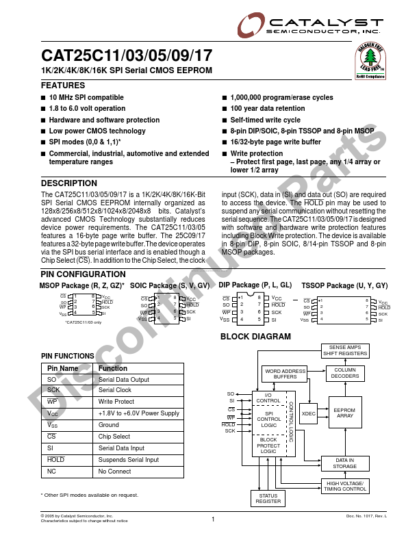
PIN CONFIGURATION
CS SO WP VSS
MSOP Package (R, Z, GZ)- SOIC Package (S, V, GV)
1 2 3 4 8 7 6 5
HOLD SCK SI
- CAT25C11/03 only
PIN FUNCTIONS Pin Name
SO SCK WP
VCC VSS CS SI i D c s
Ground
Function
Serial Data Output i t n o
CS SO WP VSS 1 2 3 4 8 7 6 5 VCC
..
HOLD SCK SI u n
CS SO WP VSS input (SCK), data in (SI) and data out (SO) are required to access the device. The HOLD pin may be used to suspend any serial munication without resetting the serial sequence. The CAT25C11/03/05/09/17 is designed with software and hardware write protection Features including Block Write protection. The device is available in 8-pin DIP, 8-pin SOIC, 8/14-pin TSSOP and 8-pin MSOP packages. d e
8 7 6 5 VCC HOLD SCK SI a P
CS SO WP VSS 1 2 3 4 s t r
8 7 6 5 VCC HOLD SCK SI
DIP Package (P, L, GL)
1 2 3 4
TSSOP Package (U, Y, GY)
BLOCK DIAGRAM
SENSE AMPS SHIFT REGISTERS
WORD ADDRESS...