FEATURES
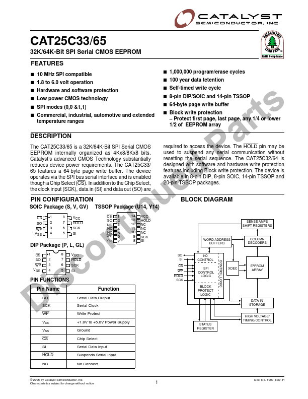
s 10 MHz SPI compatible s 1.8 to 6.0 volt operation s Hardware and software protection s Low power CMOS technology s SPI modes (0,0 &1,1) s Commercial, industrial, automotive and extended s 1,000,000 program/erase cycles s 100 year data tetention s Self-timed write cycle s 8-pin DIP/SOIC and 14-pin TSSOP s 64-byte page write buffer s Block write protection temperature ranges – Protect first page, last page, any 1/4 or lower 1/2 of EEPROM array DESCRIPTION
Catalyst’s advanced CMOS Technology substantially reduces device power requirements. In addition to the Chip Select, the clock input (SCK), data in (SI) and data out (SO) are PIN CONFIGURATION SOIC Package (S, V, GV) CS SO WP VSS 1 2 3 4 8 7 6 5 VCC HOLD SCK SI DIP Package (P, L, GL) CS SO WP VSS 1 2 3 4 8 7 6 5 VCC HOLD SCK SI PIN FUNCTIONS Pin Name SO SCK WP i D VCC VSS CS SI HOLD NC c s Ground i t n o CS SO NC NC NC WP VSS TSSOP Package (U14, Y14) 1 2 3 4 5 6 7 14 13 12 11 10 9 8 VCC HOLD NC NC NC SCK SI u n required to access the device. Catalyst Semiconductor