CFK2162-P5
CFK2162-P5 is Power GaAs FET manufactured by Celeritek.
Features t High Gain t +34 d Bm Power Output t Proprietary Power FET Process t >45% Linear Power Added Efficiency t +29 d Bm with 30 d Bc Third Order Products t Surface Mount SO-8 Power Package Applications t ISM Band Base Stations and Terminals t PCS/PCN Base Stations and Terminals t Wireless Local Loop Description
The CFK2162-P5 is a high-gain FET intended for driver amplifier applications in high-power systems, and output stage usage in medium power applications at power levels up to +34 d Bm. The device is easily matched and provides excellent
2.3 to 2.5 GHz +34 d Bm Power Ga As FET
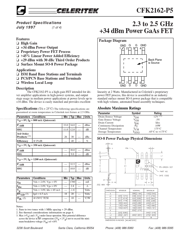
Package Diagram
G GND GND G 1 2 3 4
Back Plane is Source
8 7 6 5 D GND GND D linearity at 2 Watts. Manufactured in Celeritek’s proprietary power FET process, this device is assembled in an industry standard surface mount SO-8 power package that is patible with high volume, automated board assembly techniques.
Specifications (TA = 25°C) The following specifications are guaranteed at room temperature in Celeritek test fixture at 2.5 GHz.
Parameters
..
Absolute Maximum Ratings
Parameter Symbol Rating
Conditions
Min
Typ
Max
Units
Vd = 8V, Id = 800 m A (Quiescent) P-1d B SSG 3rd Order Products (1) Efficiency @ P1d B Vd = 5V, Id = 350 m A (Quiescent) P-1d B SSG Vd = 5V, Id = 1200 m A (Quiescent) P-1d B SSG
33.0 34.0 11.0 12.0 26
- -
- 30 40 30.0 9.0
- -
- -
- - d Bm d B d Bc % d Bm d B
Drain-Source Voltage Gate-Source Voltage Drain Current Continuous Dissipation Channel Temperature Storage Temperature
VDS VGS IDS PT TCH TSTG
12V (3) -5V Idss 10W 175°C -65°C to +175°C
SO-8 Power Package Physical Dimensions
- -
32.5 10.0
- - d Bm d B
Parameters
Conditions
Min
Typ
Max
Units gm Idss Vp BVGD (3) ΘJL (2)
Vds = 2.0V, Vgs = 0V Vds = 2.0V, Vgs = 0V Vds = 3.0V, Ids = 65 m A Igd = 6.5 m A @150°C TCH
- -
-...