CP310
CP310 is Small Signal Transistor NPN - High Voltage Transistor Chip manufactured by Central Semiconductor.
PROCESS
Small Signal Transistor
- High Voltage Transistor Chip
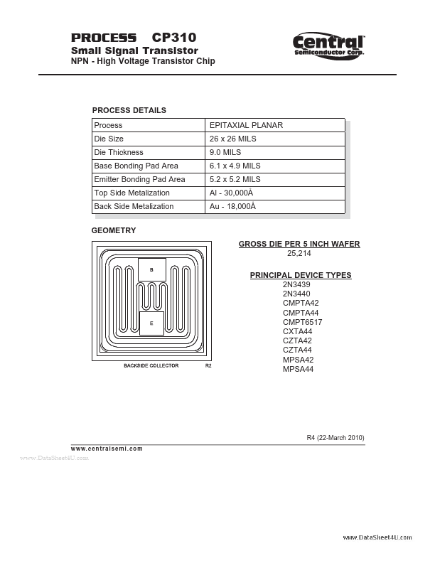
PROCESS DETAILS Process Die Size Die Thickness Base Bonding Pad Area Emitter Bonding Pad Area Top Side Metalization Back Side Metalization GEOMETRY GROSS DIE PER 5 INCH WAFER 25,214 PRINCIPAL DEVICE TYPES 2N3439 2N3440 CMPTA42 CMPTA44 CMPT6517 CXTA44 CZTA42 CZTA44 MPSA42 MPSA44 EPITAXIAL PLANAR 26 x 26 MILS 9.0 MILS 6.1 x 4.9 MILS 5.2 x 5.2 MILS Al
- 30,000Å Au
- 18,000Å
R4 (22-March 2010) w w w. c e n t r a l s e m i . c o m
..
PROCESS
Typical Electrical Characteristics
R4 (22-March 2010) w w w. c e n t r a l s e m i . c o...