CMP60N03LD13
CMP60N03LD13 is N-Channel Trench Mosfet manufactured by Champion Microelectronic.
FEATURES
Low ON Resistance Low Gate Charge Peak Current vs Pulse Width Curve Inductive Switching Curves Improved UIS Ruggedness
PIN CONFIGURATION
..
SYMBOL
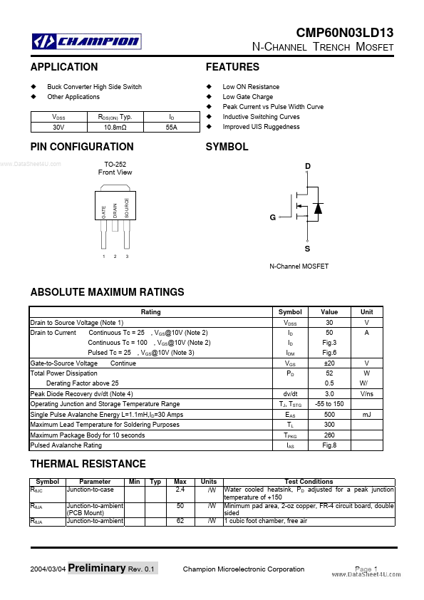
TO-252
Front View
GATE
SOURCE
DRAIN
1 2 3
N-Channel MOSFET
ABSOLUTE MAXIMUM RATINGS
Rating Drain to Source Voltage (Note 1) Drain to Current ¡Ð ¡Ð ¡Ð Continuous Tc = 25¢J , VGS@10V (Note 2) Continuous Tc = 100¢J , VGS@10V (Note 2) Pulsed Tc = 25¢J , VGS@10V (Note 3) Continue Symbol VDSS ID ID IDM VGS PD dv/dt TJ, TSTG EAS TL TPKG IAS Value 30 50 Fig.3 Fig.6 ±20 52 0.5 3.0 -55 to 150 500 300 260 Fig.8 V W W/¢J V/ns ¢J m J ¢J ¢J Unit V A
Gate-to-Source Voltage ¡Ð Total Power Dissipation
Derating Factor above 25¢J Peak Diode Recovery dv/dt (Note 4) Operating Junction and Storage Temperature Range Single Pulse Avalanche Energy L=1.1m H,ID=30 Amps Maximum Lead Temperature for Soldering Purposes Maximum Package Body for 10 seconds Pulsed Avalanche Rating
THERMAL RESISTANCE
Symbol RθJC RθJA RθJA Parameter Junction-to-case Junction-to-ambient (PCB Mount) Junction-to-ambient Min Typ Max 2.4 50 62 Units ¢J /W ¢J /W ¢J /W Test Conditions Water cooled heatsink, PD adjusted for a peak junction temperature of +150¢J Minimum pad area, 2-oz copper, FR-4 circuit board, double sided 1 cubic foot chamber, free air
2004/03/04 Preliminary Rev. 0.1
Champion Microelectronic Corporation
Page 1
N-CHANNEL TRENCH MOSFET
ORDERING INFORMATION
Part Number CMP60N03LD13 Package TO-252
ELECTRICAL CHARACTERISTICS
Unless otherwise specified, TJ = 25¢J .
..
Characteristic OFF Characteristics
Symbol VDSS £G VDSS/∆TJ IDSS
Min 30
Typ
Max
Units V
Drain-to-Source Breakdown Voltage (VGS = 0 V, ID = 250 £g A) Breakdown Voltage Temperature Coefficient,Fig.11 (Reference to 25¢J , ID = 250 £g A) Drain-to-Source Leakage Current (VDS = 24 V, VGS = 0 V, TJ = 25¢J ) (VDS = 24 V, VGS = 0 V, TJ = 125¢J ) Gate-to-Source Forward Leakage (VGS = 20 V) Gate-to-Source Reverse Leakage (VGS = -20 V) ON...