CEA3055L
CEA3055L is N-Channel Enhancement Mode Field Effect Transistor manufactured by Chino-Excel Technology.
- Part of the CEA3055L_Chino comparator family.
- Part of the CEA3055L_Chino comparator family.
N-Channel Enhancement Mode Field Effect Transistor
Features
60V, 3.7A, RDS(ON) = 100mΩ @VGS = 10V. RDS(ON) = 120mΩ @VGS = 4.5V.
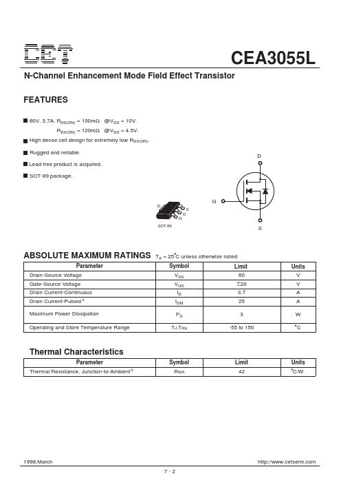
High dense cell design for extremely low RDS(ON). Rugged and reliable. Lead free product is acquired. SOT-89 package.
D...