CEB740A
CEB740A is N-Channel Enhancement Mode Field Effect Transistor manufactured by Chino-Excel Technology.
- Part of the CEB740A_Chino comparator family.
- Part of the CEB740A_Chino comparator family.
CEP740A/CEB740A CEF740A
N-Channel Enhancement Mode Field Effect Transistor
Features
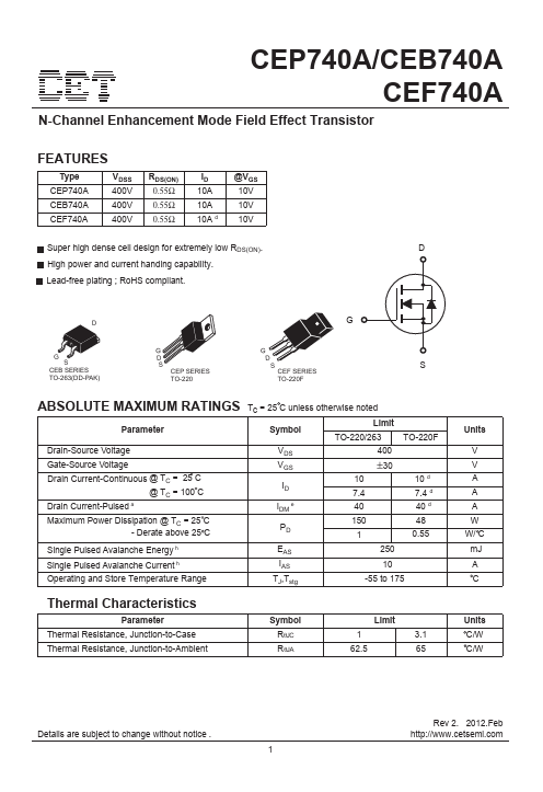
Type CEP740A CEB740A CEF740A
VDSS 400V 400V
400V
RDS(ON) 0.55Ω 0.55Ω
0.55Ω
ID 10A 10A 10A d
@VGS 10V 10V
10V
Super high dense cell design for extremely low RDS(ON). High power and current handing capability. Lead-free plating ; Ro HS pliant.
CEB SERIES TO-263(DD-PAK)
CEP SERIES TO-220
D S CEF...