CEBF630 - N-Channel Enhancement Mode Field Effect Transistor
This page provides the datasheet information for the CEBF630, a member of the CEBF630_Chino N-Channel Enhancement Mode Field Effect Transistor family.
Datasheet Summary
Features
Type CEPF630 CEBF630 CEFF630
VDSS 200V 200V
200V
RDS(ON) 0.35Ω 0.35Ω
0.35Ω
ID 10A 10A 10A d
@VGS 10V 10V
10V
Super high dense cell design for extremely low RDS(ON). High power and current handing capability. Lead free product is acquired. D
DG
GS
CEB SERIES TO-263(DD-PAK)
G D S
CEP SERIES TO-220
G
D S CEF SERIES
TO-220F
S.
CEBF640- N-Channel Enhancement Mode Field Effect Transistor
CEBFZ44- N-Channel Enhancement Mode Field Effect Transistor
CEB1012- N-Channel Enhancement Mode Field Transistor
CEB1012L- N-Channel Enhancement Mode Field Transistor
CEB4050A- N-Channel Enhancement Mode Field Transistor
CEB4050AL- N-Channel Enhancement Mode Field Effect Transistor
CEB4060- N-Channel Enhancement Mode Field Effect Transistor
Full PDF Text Transcription
Click to expand full text
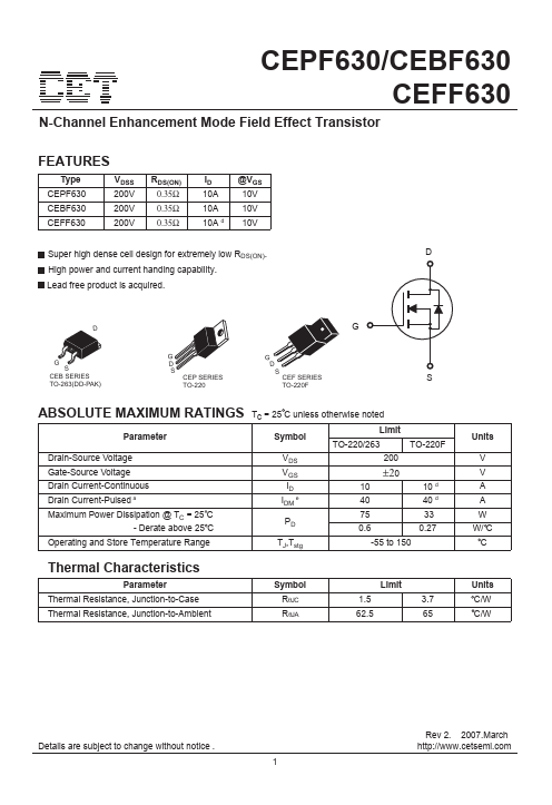
CEPF630/CEBF630 CEFF630
N-Channel Enhancement Mode Field Effect Transistor
FEATURES
Type CEPF630 CEBF630 CEFF630
VDSS 200V 200V
200V
RDS(ON) 0.35Ω 0.35Ω
0.35Ω
ID 10A 10A 10A d
@VGS 10V 10V
10V
Super high dense cell design for extremely low RDS(ON). High power and current handing capability. Lead free product is acquired.
D
DG
GS
CEB SERIES TO-263(DD-PAK)
G D S
CEP SERIES TO-220
G
D S CEF SERIES
TO-220F
S
ABSOLUTE MAXIMUM RATINGS Tc = 25 C unless otherwise noted
Parameter
Symbol
Limit
TO-220/263
TO-220F
Drain-Source Voltage Gate-Source Voltage Drain Current-Continuous Drain Current-Pulsed a Maximum Power Dissipation @ TC = 25 C
- Derate above 25 C
VDS VGS ID IDM e
PD
200
±20
10 40 75 0.6
10 d 40 d 33 0.