CEG9926
CEG9926 is Dual N-Channel Enhancement Mode Field Effect Transistor manufactured by Chino-Excel Technology.
- Part of the CEG9926_Chino comparator family.
- Part of the CEG9926_Chino comparator family.
FEATURES
20V , 4.5A , RDS(ON)=30mΩ @VGS=4.5V. RDS(ON)=40m Ω @VGS=2.5V. Super high dense cell design for extremely low RDS(ON). High power and current handing capability. TSSOP-8 for Surface Mount Package.
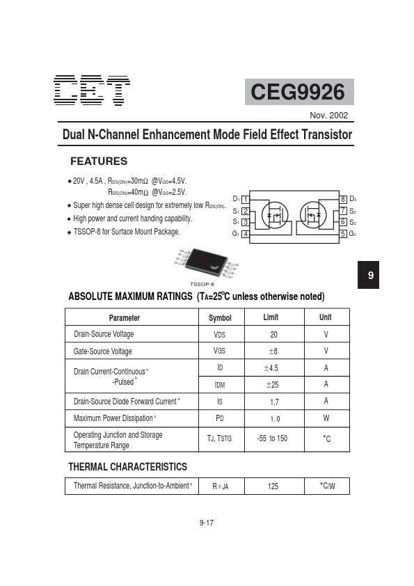
G2 S2 S2 D2
D1 1 S1 2 S1 3 G1 4
8 D2 7 S2 6 S2 5 G2
ȀȀȀ
Parameter Drain-Source Voltage Gate-Source Voltage Drain Current-Continuous a b -Pulsed Drain-Source Diode Forward Current a Maximum Power Dissipation a Operating Junction and Storage Temperature Range
G1 S1 S1 D1
TSSOP-8
ABSOLUTE MAXIMUM RATINGS (TA=25 C unless otherwise noted)
Symbol VDS VGS ID IDM IS PD TJ, TSTG Limit 20
Ć8
Ć4.5
Unit V V A A A W C
Ć25
1.7 ȑȎȐ -55 to 150
THERMAL CHARACTERISTICS
Thermal Resistance, Junction-to-Ambient a RįJA 125 C/W
9-17
ELECTRICAL CHARACTERISTICS (TA=25 C unless otherwise noted)
Parameter OFF CHARACTERISTICS
Drain-Source Breakdown Voltage Zero Gate Voltage Drain Current Gate-Body Leakage BVDSS IDSS IGSS VGS(th) RDS(ON) ID(ON) g FS
Symbol
Condition
VGS= 0V, ID=250µA VDS=20V, VGS=0V VGS=Ć8V, VDS=0V VDS=VGS, ID=250µA
VGS=4.5V, ID=4.5A VGS=4.0V, ID=5A VGS=2.5V, ID=3.5A
Min Typ C Max Unit
20 1 V µA ĆȑȐȐ n A 0.5
24 23 32
ON CHARACTERISTICS b
Gate Threshold Voltage 1.0
30 40
V mΩȀȀȀ mΩ mΩ
Drain-Source On-State Resistance On-State Drain Current Forward Transconductance
VDS=5V, VGS=4.5V VDS=10V, ID=4.5A
10 10 500 300...