Click to expand full text
P-Channel Enhancement Mode Field Effect Transistor FEATURES
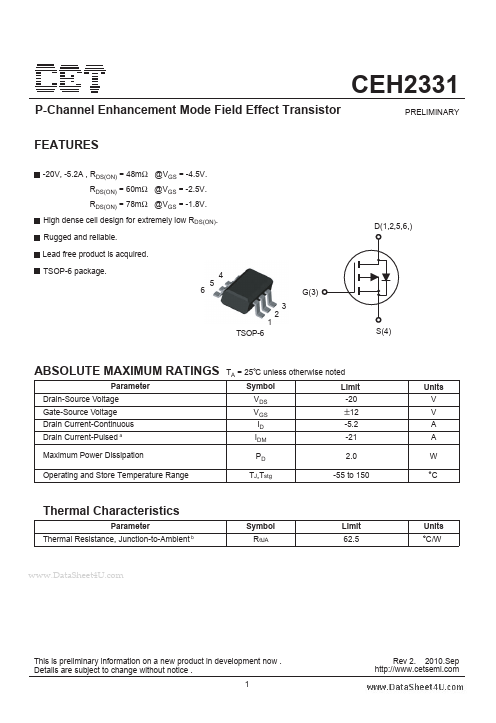
-20V, -5.2A , RDS(ON) = 48mΩ @VGS = -4.5V. RDS(ON) = 60mΩ @VGS = -2.5V. RDS(ON) = 78mΩ @VGS = -1.8V. High dense cell design for extremely low RDS(ON). Rugged and reliable. Lead free product is acquired. TSOP-6 package. 6 5 4 G(3) 1 TSOP-6 2 3
CEH2331
PRELIMINARY
D(1,2,5,6,)
S(4)
ABSOLUTE MAXIMUM RATINGS
Parameter Drain-Source Voltage Gate-Source Voltage Drain Current-Continuous Drain Current-Pulsed
a
TA = 25 C unless otherwise noted Symbol VDS VGS ID IDM PD TJ,Tstg Limit -20 Units V V A A W C
±12
-5.2 -21 2.0 -55 to 150
Maximum Power Dissipation Operating and Store Temperature Range
Thermal Characteristics
Parameter Thermal Resistance, Junction-to-Ambient b Symbol RθJA Limit 62.5 Units C/W
www.DataSheet4U.