CEM4431 Overview
Key Features
- 30V, -5.8A, RDS(ON) = 40mΩ @VGS = -10V
- RDS(ON) = 70mΩ @VGS = -4.5V
- Super high dense cell design for extremely low RDS(ON)
- High power and current handing capability
- Lead free product is acquired
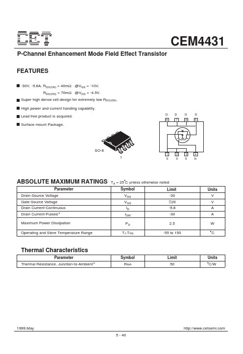
- Surface mount Package
| Part | CEM4431 |
|---|---|
| Description | P-Channel Enhancement Mode Field Effect Transistor |
| Category | Transistor |
| Manufacturer | Chino-Excel Technology |
| Size | 60.21 KB |
| Part Number | Manufacturer | Description |
|---|---|---|
| CEM4435A | CET | P-Channel Enhancement Mode Field Effect Transistor |
| CEM4435 | VBsemi | P-Channel 30V MOSFET |