Datasheet4U Logo Datasheet4U.com

CEM4936 - Dual N-Channel Enhancement Mode Field Effect Transistor

Download the CEM4936 datasheet PDF. This datasheet also covers the CEM4936_Chino variant, as both devices belong to the same dual n-channel enhancement mode field effect transistor family and are provided as variant models within a single manufacturer datasheet.

Key Features

  • 30V, 5.8A, RDS(ON) = 37mΩ @VGS = 10V. RDS(ON) = 55mΩ @VGS = 4.5V. Super high dense cell design for extremely low RDS(ON). High power and current handing capability. Lead free product is acquired. Surface mount Package. D1 D1 D2 D2 876 5 5 SO-8 1 123 4 S1 G1 S2 G2.

📥 Download Datasheet

Note: The manufacturer provides a single datasheet file (CEM4936_Chino-ExcelTechnology.pdf) that lists specifications for multiple related part numbers.

Datasheet Details

Part number CEM4936
Manufacturer Chino-Excel Technology
File Size 60.79 KB
Description Dual N-Channel Enhancement Mode Field Effect Transistor
Datasheet download datasheet CEM4936 Datasheet

Full PDF Text Transcription (Reference)

The following content is an automatically extracted verbatim text from the original manufacturer datasheet and is provided for reference purposes only.

View original datasheet text
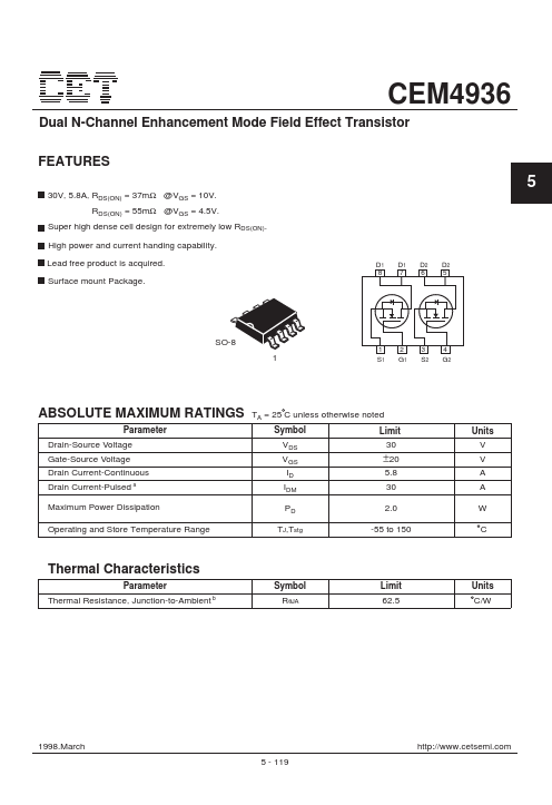
CEM4936 Dual N-Channel Enhancement Mode Field Effect Transistor FEATURES 30V, 5.8A, RDS(ON) = 37mΩ @VGS = 10V. RDS(ON) = 55mΩ @VGS = 4.5V. Super high dense cell design for extremely low RDS(ON). High power and current handing capability. Lead free product is acquired. Surface mount Package. D1 D1 D2 D2 876 5 5 SO-8 1 123 4 S1 G1 S2 G2 ABSOLUTE MAXIMUM RATINGS TA = 25 C unless otherwise noted Parameter Symbol Limit Drain-Source Voltage Gate-Source Voltage Drain Current-Continuous Drain Current-Pulsed a VDS 30 VGS ±20 ID 5.8 IDM 30 Maximum Power Dissipation PD 2.0 Operating and Store Temperature Range TJ,Tstg -55 to 150 Thermal Characteristics Parameter Thermal Resistance, Junction-to-Ambient b Symbol RθJA Limit 62.5 Units V V A A W C Units C/W 1998.