CEM6188 Description
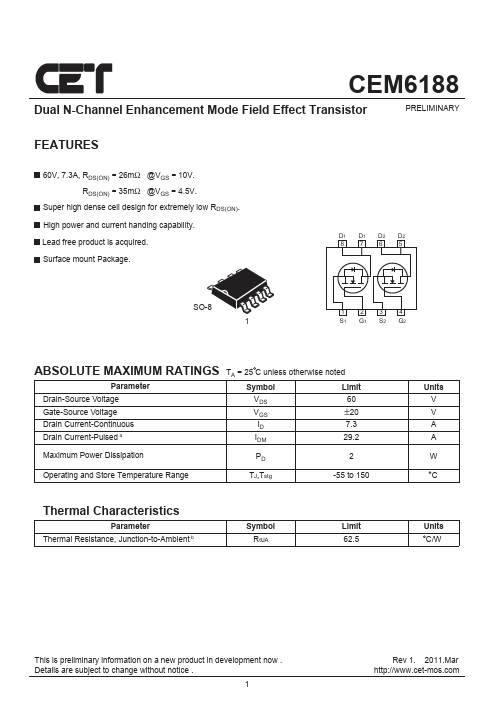
CEM6188 Dual N-Channel Enhancement Mode Field Effect Transistor PRELIMINARY.
CEM6188 is Dual N-Channel Enhancement Mode Field Effect Transistor manufactured by Chino-Excel Technology.
| Part Number | Description |
|---|---|
| CEM6186 | N-Channel Enhancement Mode Field Effect Transistor |
| CEM6056 | N-Channel Enhancement Mode Field Effect Transistor |
| CEM6086 | N-Channel Enhancement Mode Field Effect Transistor |
| CEM6086L | N-Channel Enhancement Mode Field Effect Transistor |
| CEM6088 | Dual N-Channel Enhancement Mode Field Effect Transistor |
CEM6188 Dual N-Channel Enhancement Mode Field Effect Transistor PRELIMINARY.