Datasheet4U Logo Datasheet4U.com

CEU61A3 - N-Channel MOSFET

Download the CEU61A3 datasheet PDF. This datasheet also covers the CEU61A3-Chino variant, as both devices belong to the same n-channel mosfet family and are provided as variant models within a single manufacturer datasheet.

Key Features

  • 6 30V , 40A , RDS(ON)=13.5mΩ @VGS=10V. RDS(ON)=20m Ω @VGS=4.5V. Super high dense cell design for extremely low RDS(ON). High power and current handling capability. TO-251 & TO-252 package. D G S G D S D G CEU SERIES TO-252AA(D-PAK) CED SERIES TO-251(l-PAK) S.

📥 Download Datasheet

Note: The manufacturer provides a single datasheet file (CEU61A3-Chino-ExcelTechnology.pdf) that lists specifications for multiple related part numbers.

Datasheet Details

Part number CEU61A3
Manufacturer Chino-Excel Technology
File Size 42.09 KB
Description N-Channel MOSFET
Datasheet download datasheet CEU61A3 Datasheet

Full PDF Text Transcription (Reference)

The following content is an automatically extracted verbatim text from the original manufacturer datasheet and is provided for reference purposes only.

View original datasheet text
CED61A3/CEU61A3 Jan. 2003 
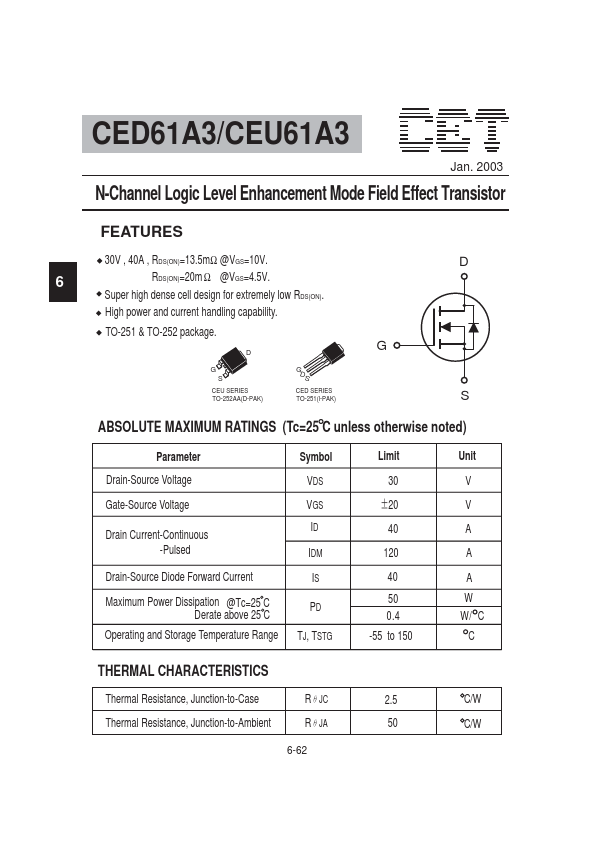
N-Channel Logic Level Enhancement Mode Field Effect Transistor FEATURES 6 30V , 40A , RDS(ON)=13.5mΩ @VGS=10V. RDS(ON)=20m Ω @VGS=4.5V. Super high dense cell design for extremely low RDS(ON). High power and current handling capability. TO-251 & TO-252 package. D G S G D S D G CEU SERIES TO-252AA(D-PAK) CED SERIES TO-251(l-PAK) S ABSOLUTE MAXIMUM RATINGS (Tc=25 C unless otherwise noted) Parameter Drain-Source Voltage Gate-Source Voltage Drain Current-Continuous -Pulsed Drain-Source Diode Forward Current Maximum Power Dissipation @Tc=25 C Derate above 25 C Operating and Storage Temperature Range Symbol VDS VGS ID IDM IS PD TJ, TSTG Limit 30 Unit V V A A A W W/ C C Ć20 40 120 40 50 0.