DESCRIPTION
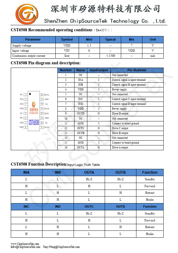
:Input Logic Truth Table 矽 S INA INB OUTA L L Hi-Z ip H L H L H L h H H L C INC IND OUTC OUTB Hi-Z L H L OUTD Function Standby Forward Retreat Brake Function L L Hi-Z Hi-Z Standby H L H L Forward L H L H Retreat H H L L Brake InFo@ChipSourceTek.com Tony.Wang@ChipSourceTek.com CST6508 Electrical characteristics: (TA=25℃,VDD=5V,RL=15Ω,unless otherwise noted) Parameter Symbol Test conditions Mini Typic Mix Unit al INA=INB=INC=IND VDD standby current IDDST =VDD=5V - 0 10 uA Output no-load INAX=H, INBX=L or INAX=L, INBX=H or VDD quiescent current IVDD 技 k Inpu tpull-down resistance Input the lowest high-level voltage Input the highest low-level voltage e Output resistance OTP temperature 科 T TSD Hysteresis RIN VINH VINL RON TSD TSDH 矽Ch源ip特Source CST6508 Typical waveform: INAX=H, INBX=H /VDD=5V` Output no-load IO=±1000mA - 220 400 uA 150 KΩ 2 V 0.8 V 0.5 Ω 165 ℃ 30 ℃ InFo@ChipSourceTek.com Tony.Wang@ChipSourceTek.com CST6508 Typical application circuit diagram: 技 ek CST6508 Special precautions: 科 T It is generally recommended to add 104 capacitors when the CST6508 power supply is connected to the ground. ChipSourceTek