ChipSourceTek MX2302A
The MX2302A uses advanced trench technology to provide excellent RDS(ON), low gate charge and operation with gate voltages as low as 2.5V. This device is suitable for use as a load switch or in PWM applications.| Part No. | MX2302A |
|---|---|
| Datasheet | MX2302A Download |
| Manufacturer |  ChipSourceTek |
| Description | N-Channel Power MOSFET |
| Buy | Stock & Price |

DESCRIPTION
MX2302AGENERAL FEATURES
Schematic● VDS =20V,ID = 3.0A
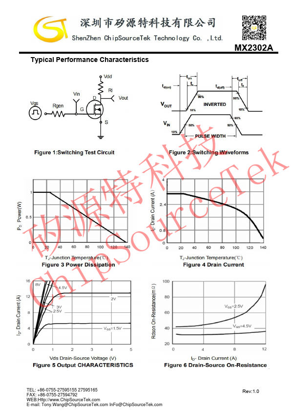
● @VGS= 4.5V RDS(ON)(Typ.)=45mΩ
● @VGS= 2.5V RDS(ON)(Typ.)=55mΩ
● High power and current handing capability 技
● Lead free product is acquired k
● Surface mount package 科 e Application
● PWM applications T
● Load switch 特 e
● Battery protection 源 rc Package u
● SOT-23 Marking and pin assignment SOT-23 (TOP VIEW) 矽 pSo Ordering Information i Part Number ChMX2302A Marking b.NC3A StorageTemperature -55°C to +150°C Package SOT-23 Devices Per Reel 3000
ABSOLUTE MAXIMUM RATINGS
(TA=25℃ unless otherwise noted) parameter Drain-source voltage Gate-source voltage Drain current-continuousa@Tj=125℃ -pulse db Maximum power dissipation Operating junction Temperature range symbol VDS VGS ID IDM PD Tj limit unit 20 V ±10 V 3 A 10 A 1 W -55—125 ℃ TEL: +86-0755-27595155 27595165 FAX: +86-0755-27594792 WEB: E-mail: Tony.Wang@ChipSourceTek.com InFo@ChipSourceTek.com Rev:1.0 v:1.0 MX2302AELECTRICAL CHARACTERISTICS
(TA=25℃ unless otherwise...