ChipSourceTek MX3407
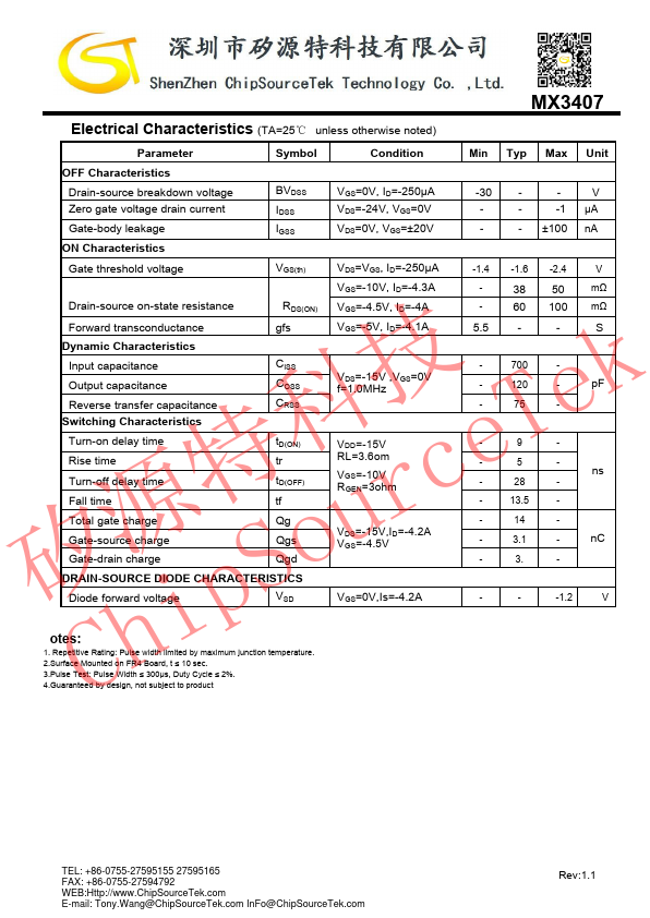
This device is suitable for use as a load switch or in PWM applications.| Part No. | MX3407 |
|---|---|
| Datasheet | MX3407 Download |
| Manufacturer |  ChipSourceTek |
| Description | P-Channel Enhancement Mode Power MOSFET |
| Buy | Stock & Price |
DESCRIPTION
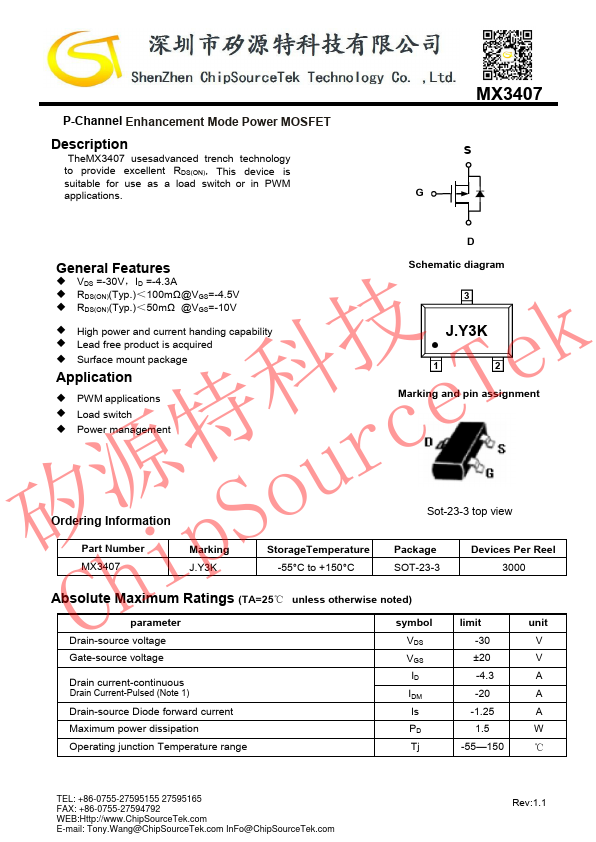
TheMX3407 usesadvanced trench technology to provide excellent RDS(ON), MX3407 s G DGENERAL FEATURES
Schematic diagram● VDS =-30V,ID =-4.3A
● RDS(ON)(Typ.)<100mΩ@VGS=-4.5V 3
● RDS(ON)(Typ.)<50mΩ @VGS=-10V
● High power and current handing capability
● Lead free product is acquired 技 k
● Surface mount package e Application 科 T
● PWM applications
● Load switch e
● Power management J.Y3K 1 2 Marking and pin assignment 源特 ourc Ordering Information 矽 S Part Number p MX3407 Marking J.Y3K Sot-23-3 top view StorageTemperature -55°C to +150°C Package SOT-23-3 Devices Per Reel 3000 i
ABSOLUTE MAXIMUM RATINGS
(TA=25℃ unless otherwise noted) Chparameter symbol limit unit Drain-source voltage VDS -30 V Gate-source voltage VGS ±20 V Drain current-continuous Drain Current-Pulsed (Note 1) ID -4.3 A IDM -20 A Drain-source Diode forward current Is -1.25 A Maximum power dissipation PD 1.5 W Operating junction Temperature range Tj -55—150 ℃ TEL: +86-0755-27595155 27595165 FAX: +86-0755-2759479...