MXDW01
Description
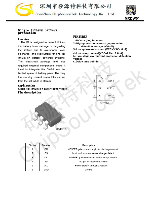
MOSFET gate connection pin for discharge control Input pin for current sense, charger detect MOSFET gate connection pin for charge control Test pin for reduce delay time 5 VCC Power supply, through a resistor 6 GND Ground MXDW01 Single lithium battery protection Parameter Symbol Ratings Unit Input voltage between VCC and VCC GND-0.3 to GND+10 V OC output pin voltage VOC VCC -24 to VCC +0.3 V OD output pin voltage VOD GND-0.3 to VCC +0.3 V CS input pin voltage VCS VCC -24 to VCC +0.3 V Operating Temperature Range TOP -40 to +85 °C Storage Temperature Range TST -40 to +125 °C C矽h源ipS特o科ur技ceTek TypicalApplication MXDW01 Test Symbol Condition Min.
Key Features
- The very low standby current drains little current 技 from the cell while in storage
- k application Single-cell lithium-ion battery/battery pack 科 e Pin description 矽源ipS特ourceT PinNo
- 1 2 h3 C4 Symbol OD CS OC TD