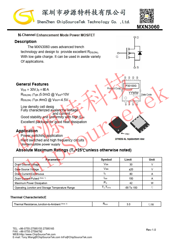
DESCRIPTION
It can be used in awide variety Of applications. MXN3060 GENERAL FEATURES
VDS = 30V,ID = 80 A RDS(ON) (Typ.)5.0mΩ @ VGS=10V 技 RDS(ON) (Typ.)6mΩ @ VGS=-4.5V k Low density cell desig 科 e Fully characterized avalanche voltage T and current Good stability and uniformity with high EAS 特 e Excellent package for good heat dissipation P30100G c Application 源 r Power switching application u Hard switched and high frequency circuits Uninterruptible power supply 矽 o ABSOLUTE MAXIMUM RATINGS
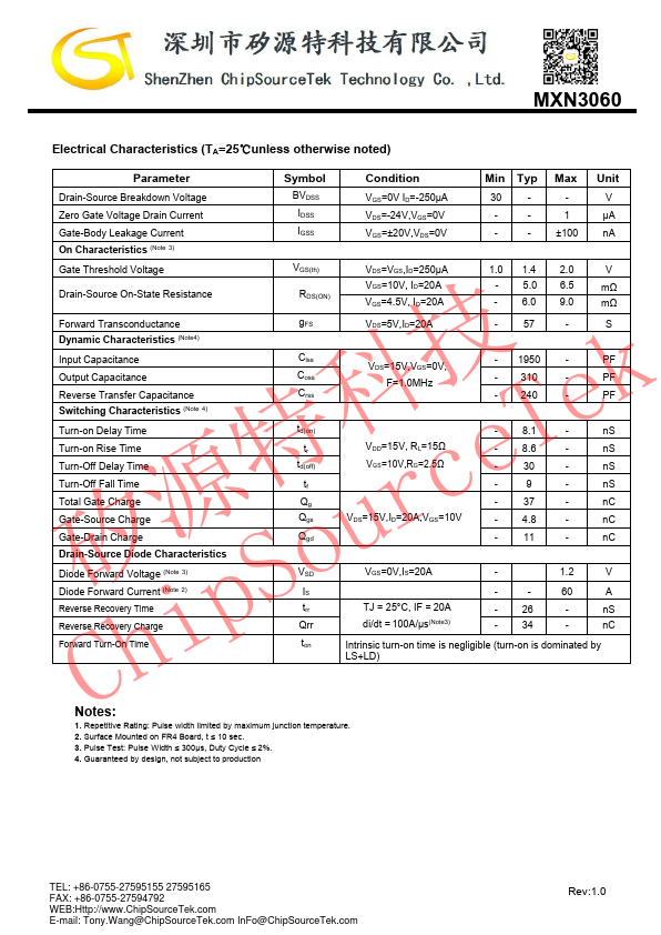
(TA=25℃unless otherwise noted) pS Parameter Drain-Source Voltage i Gate-Source Voltage h Drain Current-Continuous CDrain Current-Pulsed (Note 1) Symbol VDS VGS ID IDM Limit 30 ±20 80 150 Unit V V A A Maximum Power Dissipation PD 42 W Operating Junction and Storage Temperature Range TJ,TSTG -55 To 150 ℃ Thermal CharacteristicE Thermal Resistance,Junction-to-Ambient (Note 2) RθJA 3.0 ℃/W TEL: +86-0755-27595155 27595165 FAX: +86-0755-27594792 WEB: E-mail: Tony.Wang@ChipSourceTek.com InFo@ChipSourceTek... ChipSourceTek