APPLICATIONS
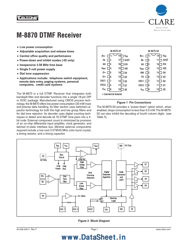
include: telephone switch equipment, remote data entry, paging systems, personal computers, credit card systems Manufactured using CMOS process technology, the M-8870 offers low power consumption (35 mW max) and precise data handling. External component count is minimized by provision of an on-chip differential input amplifier, clock generator, and latched tri-state interface bus. Minimal external components required include a low-cost 3.579545 MHz color burst crystal, a timing resistor, and a timing capacitor. Figure 1 Pin Connections The M-8870-02 provides a “power-down” option which, when enabled, drops consumption to less than 0.5 mW. The M-887002 can also inhibit the decoding of fourth column digits (see Table 5). Figure 2 Block Diagram 40-406-00011, Rev. F Page 1 M-8870 Functional DESCRIPTION
M-8870 operating functions (see Figure 2) include a bandsplit filter that separates the high and low tones of the received pair, and a digital decoder that verifies both the frequency and duration of the received tones before passing the resulting 4-bit code to the output bus. Clare