GENERAL DESCRIPTION
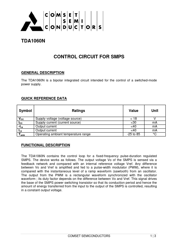
QUICK REFERENCE DATA Symbol VCC ICC -I14 I15 Tamb Ratings Supply voltage (voltage source) Supply current (current source) Output current Output current Operating ambiant temperature range Value < 18 <30 <40 <40 -25 to 85 Unit V mA mA mA °C FUNCTIONAL DESCRIPTION
The TDA1060N contains the control loop for a fixed-frequency pulse-duration regulated SMPS. The device works as follows. The output voltage Vo of the SMPS is sensed via a feedback network and compared with an internal reference voltage Vref. Any difference between Vo and Vref is amplified and fed to a pulse-width modulator (PWM), where it is compared with the instantaneous level of a ramp waveform (sawtooth) from an oscillator. The output from the PWM is a rectangular waveform synchronized with the oscillator waveform ; its duty factor depends on the difference between Vo and Vref. This signal drives the base of the SMPS power switching transistor so that its conduction period and hence the amount of energy transferred from the input to the output of the SMPS is controlled, resulting in a constant output voltage. Comset Semiconductor