Convert SemiConductor CS2N100D
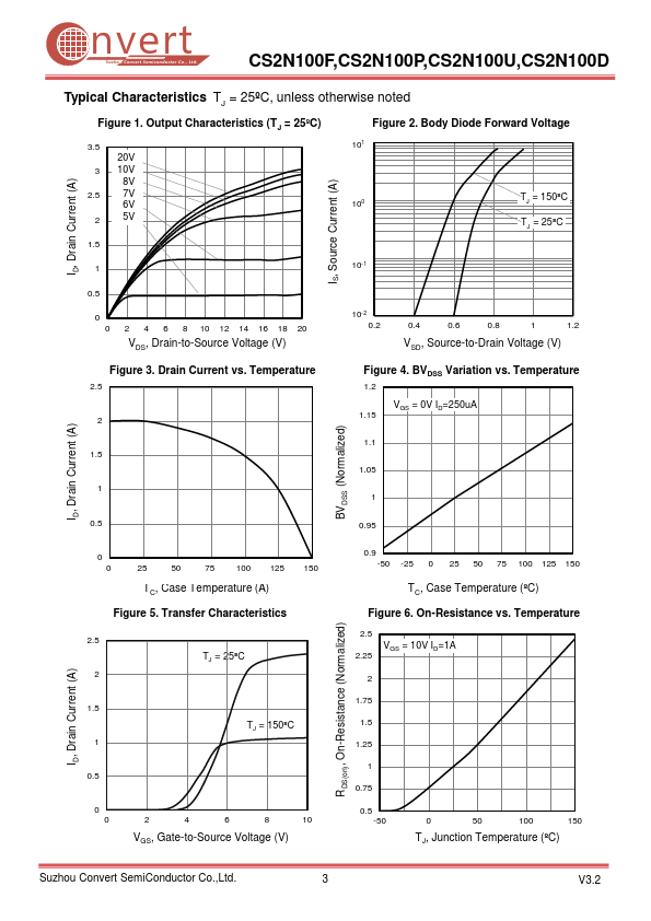
CS2N100D IS, Source Current (A) ID, Drain Current (A) Typical Characteristics TJ = 25ºC, unless otherwise noted Figure 1.| Part No. | CS2N100D |
|---|---|
| Datasheet | CS2N100D Download |
| Manufacturer | Convert SemiConductor |
| Description | 1000V N-Channel MOSFET |
| Buy | Stock & Price |
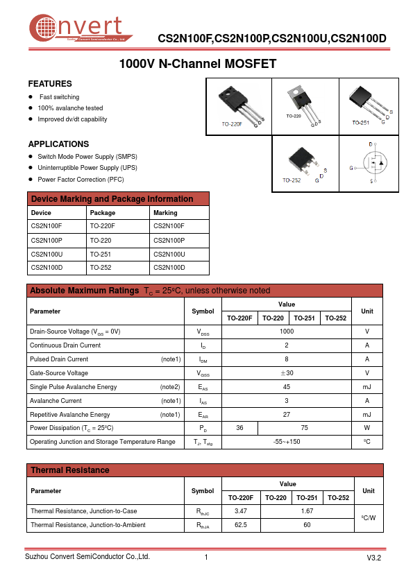
FEATURES
● Fast switching● 100% avalanche tested
● Improved dv/dt capability
APPLICATIONS
● Switch Mode Power Supply (SMPS)● Uninterruptible Power Supply (UPS)
● Power Factor Correction (PFC) Device Marking and Package Information Device Package Marking CS2N100F TO-220F CS2N100F CS2N100P TO-220 CS2N100P CS2N100U TO-251 CS2N100U CS2N100D TO-252 CS2N100D
ABSOLUTE MAXIMUM RATINGS
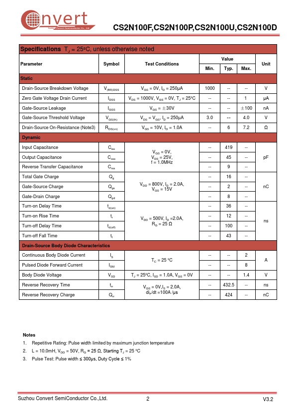
TC = 25ºC, unless otherwise noted Parameter Value Symbol Unit TO-220F TO-220 TO-251 TO-252 Drain-Source Voltage (VGS = 0V) VDSS 1000 V Continuous Drain Current ID 2 A Pulsed Drain Current (note1) IDM 8 A Gate-Source Voltage VGSS ±30 V Single Pulse Avalanche Energy (note2) EAS 45 mJ Avalanche Current (note1) IAS 3 A Repetitive Avalanche Energy (note1) EAR 27 mJ Power Dissipation (TC = 25ºC) PD 36 75 W Operating Junction and Storage Temperature Range TJ, Tstg -55~+150 ºC Thermal Resistance Parameter Thermal Resistance, Junction-to-Case Thermal Resistance, Junction-to-Ambient Symbol RthJC RthJA TO-220F 3.47 62.5 Value TO-220 TO-251 TO-252 1.67 60 Unit ºC/W Suzhou Convert SemiConductor Co.,Ltd.