GENERAL DESCRIPTION
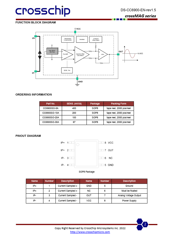
Customers can easily complete their PCB design and implementation. The CC6900 device consists of a precise, low-offset, linear Hall circuit with a copper conduction path located near the surface of the die. When current flows through the copper conduction path, a magnetic field generates. Meanwhiles the Hall circuit converts this magnetic signal to output voltage signal. The Hall circuit based on BiCOMS process integrates a high sensitivity Hall element, oscillator, Hall signal pre-amplifier, temperature compensation circuit, dynamic offset cancellation circuit, sensitivity trimming circuit and output amplifier. The temperature compensation circuit ensures good temperature stability of CC6900. Chopper stabilization technique is applied to the Hall circuit to minimize offset voltage. High chopping frequency up to 1MHz makes CC6900 80kHz bandwidth and ultra-short step input response time down to typical 2us. Because of this chopper stabilization approach, the output voltage from the Hall IC is desensitized to the effects of temperature and mechanical stress.