AN165
AN165 is EMI REDUCTION TECHNIQUES manufactured by Crystal.
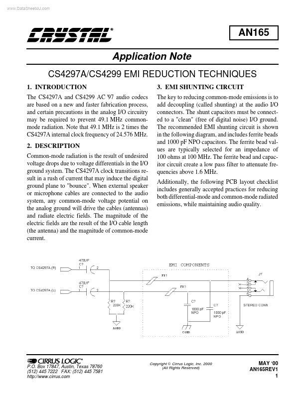
DESCRIPTION mon-mode radiation is the result of undesired voltage drops due to voltage differentials in the I/O ground system. The CS4297A clock transitions result in a rush of current that may induce the digital ground plane to "bounce". When external speaker or microphone cables are connected to the audio system, any mon-mode voltage potential on the analog ground will drive the cables (antennas) and radiate electric fields. The magnitude of the electric fields are the result of the I/O cable length (the antenna) and the magnitude of mon-mode current.
P.O. Box 17847, Austin, Texas 78760 (512) 445 7222 FAX: (512) 445 7581 http://.cirrus.
Copyright © Cirrus Logic, Inc. 2000 (All Rights Reserved)
MAY ‘00 AN165REV1 1
4. PCB LAYOUT CHECKLIST
- Connect analog and digital ground together with a 1/16 inch trace under the CS4297A. A direct connection between analog and digital ground will reduce the differential-mode radiation and improve the EOS (Electrical Overstress) capabilities of the CS4297A. Construct a "clean" chassis ground on the PCB around the I/O connectors, and connect the I/O ground to the system frame ground. Connect chassis ground to digital ground in a quiet area, away from the CS4297A. The ferrite bead and decoupling capacitor bination shown in the block diagram on page one of this document, form a low-pass filter to remove the mon-mode voltages. The de- coupling capacitor must be terminated to a clean (free of digital noise) I/O chassis ground. A separate analog ground return path between the I/O connectors and analog ground plane must be maintained to reduce loop areas.
- Chassis and analog planes should be identical on all layers, and the gap or "moat" between planes should be 1/8 inch to prevent coupling between planes. The absolute minimum moat spacing is 1/16 inch. Do not overlap digital and...