FEATURES
► Positive gain slope ► High isolation ► Fast switching speed ► Non-reflective design ► Small die size DESCRIPTION
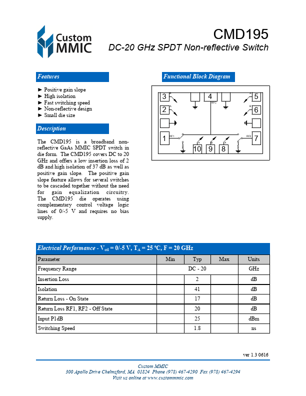
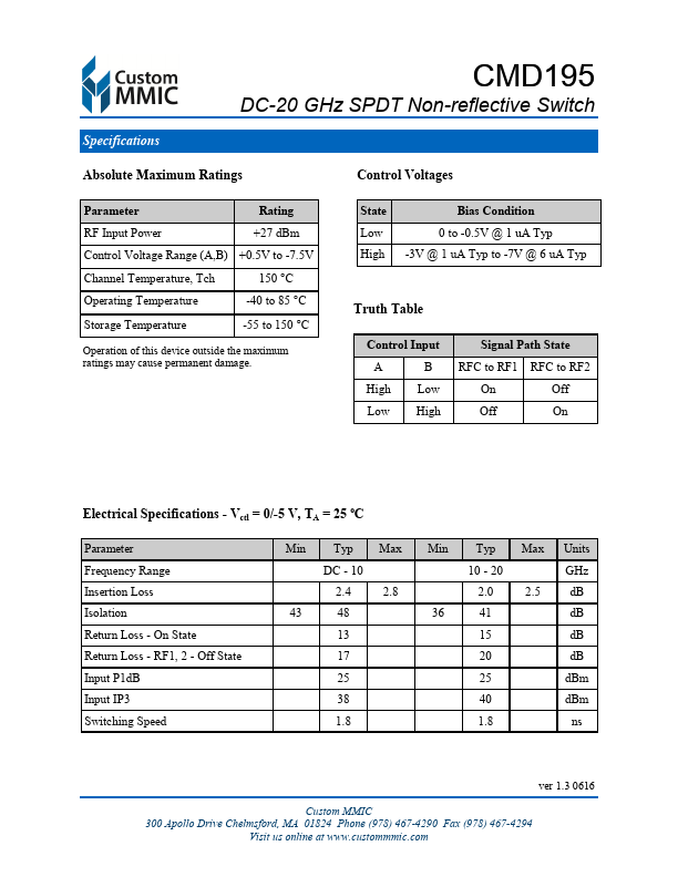
The CMD195 die operates using complementary control voltage logic lines of 0/-5 V and requires no bias supply. Functional Block Diagram 3B A 2 4 RFC 5A B 6 1 RF1 AB A 10 9 8 7RF2 Electrical Performance - Vctl = 0/-5 V, TA = 25 oC, F = 20 GHz Parameter Min Typ Frequency Range DC - 20 Insertion Loss 2 Isolation 41 Return Loss - On State 17 Return Loss RF1, RF2 - Off State 20 Input P1dB 25 Switching Speed 1.8 Max Units GHz dB dB dB dB dBm ns ver 1.3 0