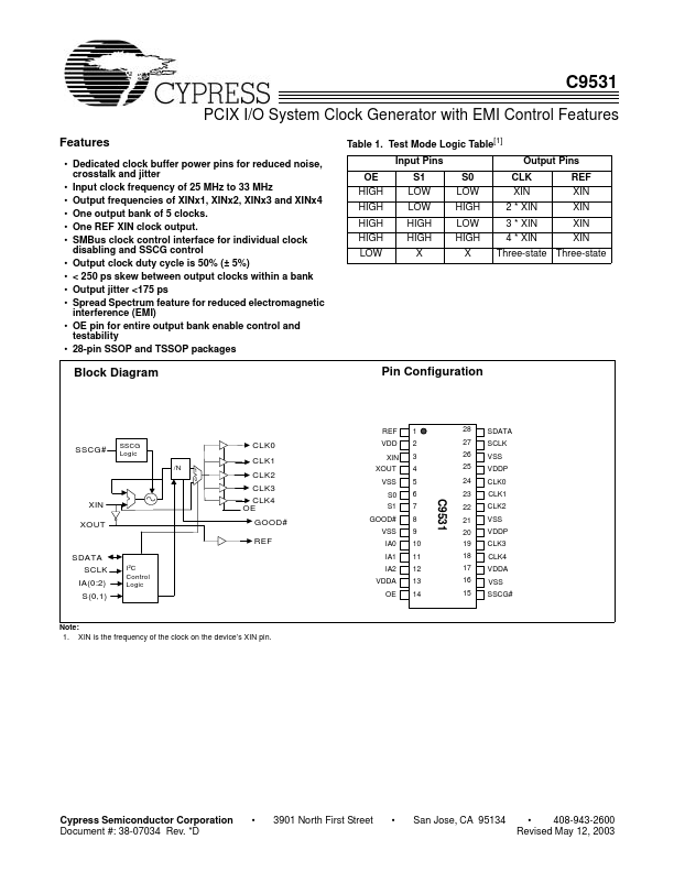
Datasheet4U Logo Datasheet4U.com

C9531 - PCIX I/O System Clock Generator with EMI Control Features

Datasheet Summary

Description

3] Pin[2] 3 4 1 14

24, 23, 22, 19, 18 8 XIN XOUT REF OE CLK(0:4) GOOD# Name PWR[4] VDDA VDDA VDD VDD VDDP VDD I/O I O O I O O Description Crystal Buffer Input Pin.

Connects to a crystal, or an external clock source.

Serves as input clock TCLK, in Test mode.

Features

  • Features.
  • Dedicated clock buffer power pins for reduced noise, crosstalk and jitter.
  • Input clock frequency of 25 MHz to 33 MHz.
  • Output frequencies of XINx1, XINx2, XINx3 and XINx4.
  • One output bank of 5 clocks.
  • One REF XIN clock output.
  • SMBus clock control interface for individual clock disabling and SSCG control.
  • Output clock duty cycle is 50% (± 5%).
  • < 250 ps skew between output clocks within a bank.
  • Output jitte.

📥 Download Datasheet

Datasheet preview – C9531

Datasheet Details

Part number C9531
Manufacturer Cypress Semiconductor
File Size 115.60 KB
Description PCIX I/O System Clock Generator with EMI Control Features
Datasheet download datasheet C9531 Datasheet
Additional preview pages of the C9531 datasheet.
Other Datasheets by Cypress Semiconductor

Full PDF Text Transcription

Click to expand full text
C9531 PCIX I/O System Clock Generator with EMI Control Features Features • Dedicated clock buffer power pins for reduced noise, crosstalk and jitter • Input clock frequency of 25 MHz to 33 MHz • Output frequencies of XINx1, XINx2, XINx3 and XINx4 • One output bank of 5 clocks. • One REF XIN clock output. • SMBus clock control interface for individual clock disabling and SSCG control • Output clock duty cycle is 50% (± 5%) • < 250 ps skew between output clocks within a bank • Output jitter <175 ps • Spread Spectrum feature for reduced electromagnetic interference (EMI) • OE pin for entire output bank enable control and testability • 28-pin SSOP and TSSOP packages Table 1.
Published: |