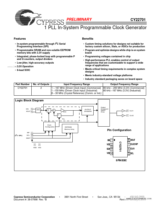
CY22701 Overview
Pin 7 is configured as Write Protect (see “Write Protect (WP) Registers” section on page 5 to configure as CLK2) This default clock configuration is typically customized to meet the needs of a specific application. It provides a clock signal upon power-on, to facilitate in-system programming. Alternatively, the CY22701 may be programmed with a different clock configuration prior to placement of the CY22701 in...
CY22701 Key Features
- In-system programmable through I2C Serial Programming Interface (SPI)
- Programmable SRAM and non-volatile EEPROM memory bits with 3.3V supply
- Integrated, phase-locked loop with programmable P and Q counters, output dividers
- Low-jitter, high-accuracy outputs
- 3.3V Operation
- 8-lead SOIC
- Custom timing solutions for designs not suitable for factory custom silicon, Xtals, or ASICs for production
- Program and optimize designs while chip is on system board
- Programming voltages contained in chip
CY22701 Applications
- Meets critical timing requirements in plex system designs