CY25822-2
CY25822-2 is CK-SSC Spread Spectrum Clock Generator manufactured by Cypress.
Features
- -
- -
- -
- 3.3V operation 48- and 66-MHz frequency support Selectable slew rate control 350-p S jitter I2C programmability 500-µA power-down current Spread Spectrum for best electromagnetic interference (EMI) reduction
- 8-pin SOIC package
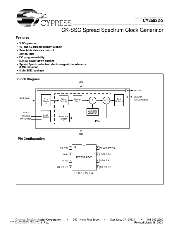
Block Diagram
REFOUT CLKOUT (SSCG Output)
Clock Input
Freq. Divider M
Phase Detector
Charge Pump
Σ
Post Dividers
SDATA SCLOCK PWRDWN# Logic Control Feedback Divider N
Modulating Waveform
Pin Configuration
C L K IN 1 VDD 2 8
- P W R D W N # 7 SC LO C K
C Y 2 5 8 2 2 -2
GND 3 C LKO U T 4
- 1 5 0 K Ω P u ll-u p 6 SDATA 5 REFOUT
Cypress Semiconductor Corporation Document #: 38-07531 Rev.
- -
- 3901 North First Street
- San Jose, CA 95134
- 408-943-2600 Revised March 18, 2003
..
Pin Description
Pin No. 1 2 3 4 5 6 7 8 Pin Name CLKIN VDD GND CLKOUT REFOUT SDATA SCLOCK PWRDWN# Pin Type Input Power Ground Output Output I/O Input Output Pin Description
48-MHz or 66-MHz Clock Input. Power Supply for PLL and Outputs. Ground for Outputs. 48-MHz or 66-MHz Spread Spectrum Clock Output. Non-spread Spectrum Reference Clock Output. I2C-patible SDATA. I2C-patible SCLOCK. LVTTL Input for Power Down# Active Low.
Serial Data Interface
To enhance the flexibility and function of the clock synthesizer, a two-signal serial interface is provided. Through the Serial Data Interface, various device functions such as individual clock output buffers, etc., can be individually enabled or disabled. The registers associated with the Serial Data Interface initializes to their default setting upon power-up, and therefore use of this interface is optional. Clock device register changes are normally made upon system initialization, if any are required. The interface can also be used during system operation for power management functions. Table 1. mand Code Definition Bit 7 0 = Block read or block write operation 1 = Byte read or byte write operation
Data Protocol
The clock driver serial protocol accepts byte...