Datasheet4U Logo Datasheet4U.com

CY28341 - Universal Single-Chip Clock Solution

General Description

Pin 3 4 1 XIN XOUT FS0/REF0 VDD VDD Name PWR I/O I O Description Oscillator Buffer Input.

Connect to a crystal or to an external clock.

Oscillator Buffer Output.

Key Features

  • Supports VIA P4M266/KM266 chipsets Supports Pentium® 4, Athlon™ processors Supports two DDR DIMMS Supports three SDRAMS DIMMS at 100 MHz Provides:.
  • Two different programmable CPU clock pairs.
  • Six differential SDRAM DDR pairs.
  • Three low-skew/low-jitter AGP clocks.
  • Seven low-skew/low-jitter PCI clocks.
  • One 48M output for USB.
  • One programmable 24M or 48M for SIO.
  • Dial-a-Frequency™ and D.

📥 Download Datasheet

Full PDF Text Transcription (Reference)

The following content is an automatically extracted verbatim text from the original manufacturer datasheet and is provided for reference purposes only.

View original datasheet text
CY28341 
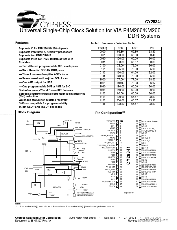
Universal Single-Chip Clock Solution for VIA P4M266/KM266 DDR Systems Features • • • • • Supports VIA P4M266/KM266 chipsets Supports Pentium® 4, Athlon™ processors Supports two DDR DIMMS Supports three SDRAMS DIMMS at 100 MHz Provides: — Two different programmable CPU clock pairs — Six differential SDRAM DDR pairs — Three low-skew/low-jitter AGP clocks — Seven low-skew/low-jitter PCI clocks — One 48M output for USB — One programmable 24M or 48M for SIO • Dial-a-Frequency™ and Dial-a-dB features • Spread Spectrum for best electromagnetic interference (EMI) reduction • Watchdog feature for systems recovery • SMBus-compatible for programmability • 56-pin SSOP and TSSOP packages Table 1.