CY2XL11
Key Features
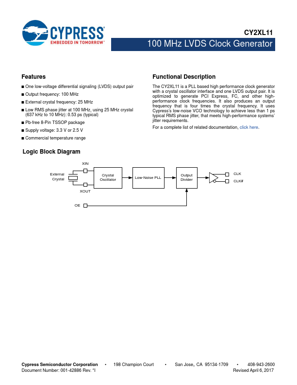
- Functional Description
- 8-Pin TSSOP Pin Number 1, 8 2 3, 4 5 6,7 Pin Name VDD VSS XOUT, XIN OE CLK#, CLK I/O Type Power Power XTAL output and input CMOS input LVDS output Ground Parallel resonant crystal interface Output enable. When HIGH, the output is enabled. When LOW, the output is high-impedance Differential clock output Description 3.3 V or 2.5 V power supply. All supply current flows through pin 1