CY5057
CY5057 is High-Frequency Flash Programmable PLL Die manufactured by Cypress.
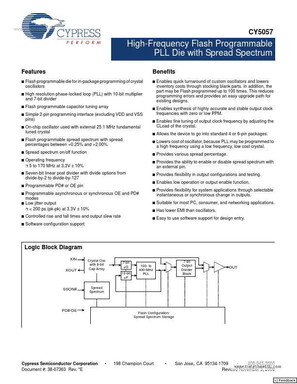
..
High-Frequency Flash Programmable PLL Die with Spread Spectrum
Features
- -
- -
- -
- -
Benefits
- Flash programmable die for in-package programming of crystal oscillators High resolution phase-locked loop (PLL) with 10-bit multiplier and 7-bit divider Flash programmable capacitor tuning array Simple 2-pin programming interface (excluding VDD and VSS pins) On-chip oscillator used with external 25.1 MHz fundamental tuned crystal Flash programmable spread spectrum with spread percentages between +0.25% and +2.00% Spread spectrum on/off function Operating frequency
- 5 to 170 MHz at 3.3V ± 10% Seven-bit linear post divider with divide options from divide-by-2 to divide-by-127 Programmable PD# or OE pin
Enables quick turnaround of custom oscillators and lowers inventory costs through stocking blank parts. In addition, the part may be Flash programmed up to 100 times. This reduces programming errors and provides an easy upgrade path for existing designs. Enables synthesis of highly accurate and stable output clock frequencies with zero or low PPM. Enables fine tuning of output clock frequency by adjusting the CLoad of the crystal. Allows the device to go into standard 4 or 6-pin packages. Lowers cost of oscillator, because PLL may be programmed to a high frequency using a low frequency, low cost crystal. Provides various spread percentage. Provides the ability to enable or disable spread spectrum with an external pin. Provides flexibility in output configurations and testing. Enables low operation or output enable function. Provides flexibility for system applications through selectable instantaneous or synchronous change in outputs. Suitable for most PC, consumer, and networking applications. Has lower EMI than oscillators. Easy to use software support for design entry.
- -
- -
- -
- -
- -
- -
- -
- Programmable asynchronous or synchronous OE and PD# modes
- Low jitter output
- < 200 ps (pk-pk) at 3.3V ± 10%
- -
Controlled rise and...